Covering method and organic EL element manufacturing method
a manufacturing method and organic el technology, applied in the direction of organic semiconductor devices, semiconductor/solid-state device testing/measurement, electrical or functional layers with local level unevenness, etc., can solve the problems of forming dark spots, affecting the and affecting the stability of the organic el element, etc., to achieve the effect of high boiling point, not easy to evaporate, and increased viscosity of the mixtur
- Summary
- Abstract
- Description
- Claims
- Application Information
AI Technical Summary
Benefits of technology
Problems solved by technology
Method used
Image
Examples
embodiment 1
1.1 Overall Structure
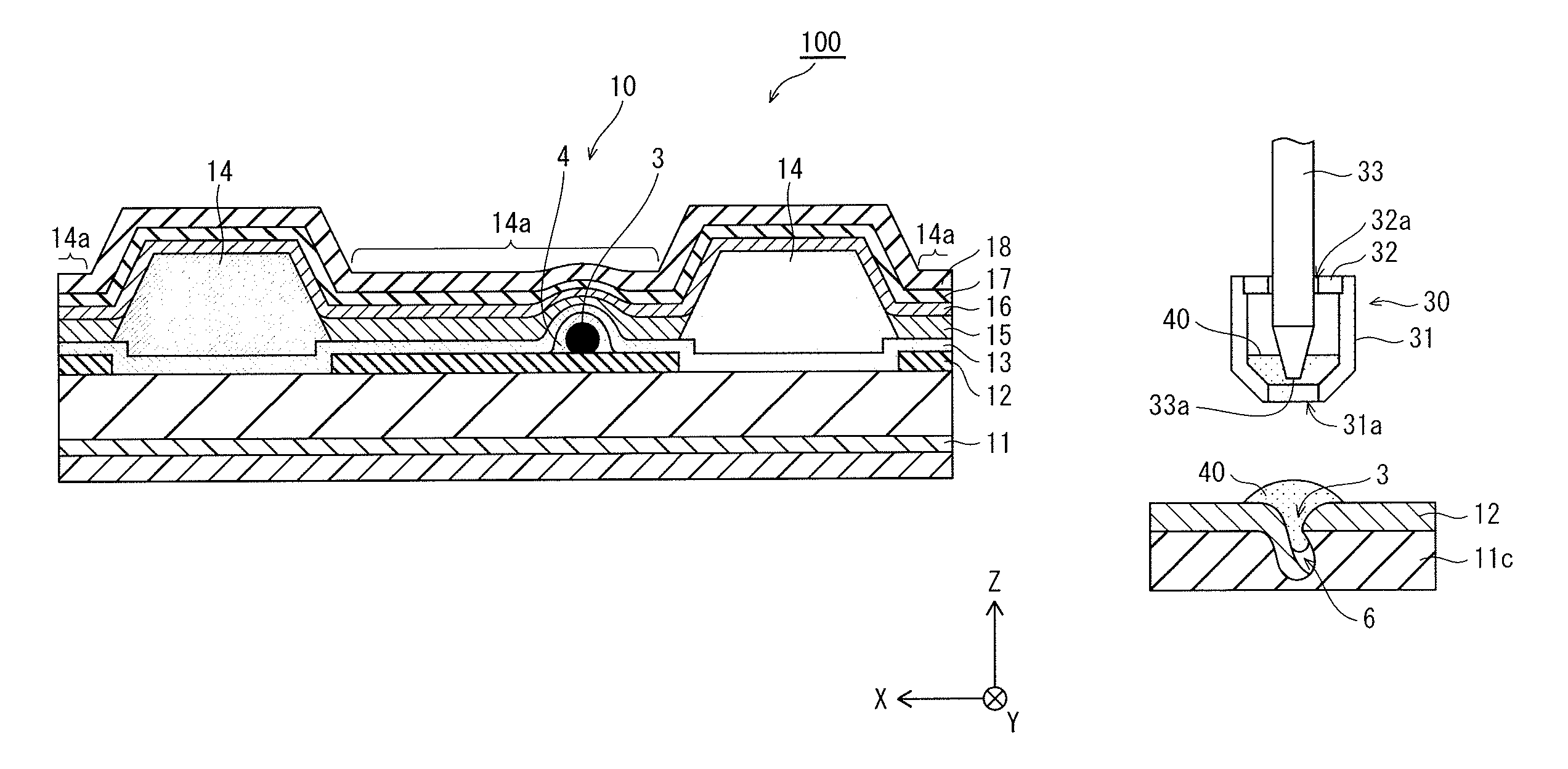
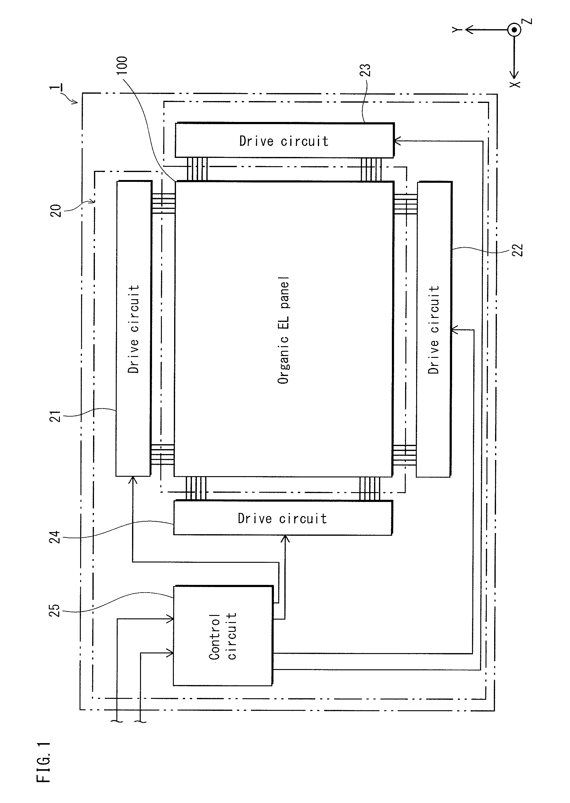
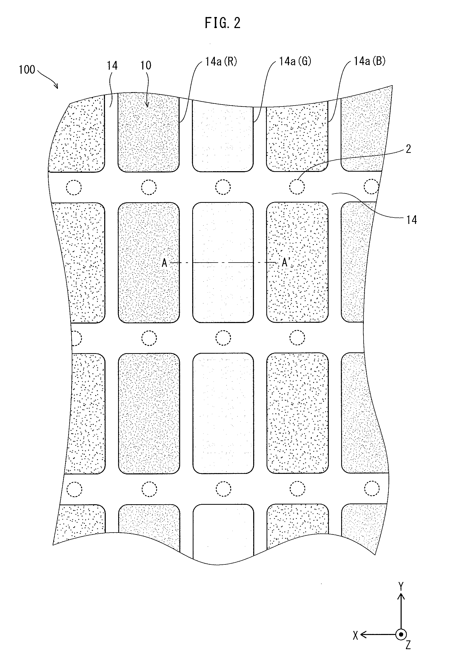
[0032]FIG. 1 is a schematic block diagram illustrating a structure of an organic EL display device 1. The organic EL display device 1 includes an organic EL display panel 100 pertaining to embodiment 1. As illustrated in FIG. 1, the organic EL display device 1 includes the organic EL display panel 100 and a drive / control unit 20 connected to the organic EL display panel 100. The organic EL display panel 100 is a panel utilizing electro-luminescence occurring in organic material. The organic EL display panel 100 includes a plurality of organic EL elements 10 (illustrated in FIGS. 2 and 3) that are disposed on a substrate and arranged, for example, to form a matrix. The drive / control unit 20 includes four drive circuits, namely drive circuits 21 through 24, and a control circuit 25.
[0033]Note that when the organic EL display device 1 is actually implemented, the arrangement of the drive / control unit 20 with respect to the organic EL display panel 100 may differ fr...
embodiment 2
[0124]In embodiment 1, the defective portion 3 is a foreign particle on the pixel electrode 12. However, the defective portion 3 need not be such a foreign particle. For example, as already described in embodiment 1 in the explanation concerning the defective portion 3, an upward protrusion may be formed in the pixel electrode 12 due to a foreign particle or an upward protrusion existing lower than the pixel electrode 12, in which case the upward protrusion of the pixel electrode 12 is the defective portion 3.
[0125]In embodiment 2, description is provided on a case where the defective portion 3 is an upward protrusion of the pixel electrode 12 that is formed due to an upward protrusion formed in the surface of the interlayer insulating layer 11c.
[0126]Note that in the following, in order to avoid the repetition of description already provided in embodiment 1, constituent elements that correspond to those having been described in embodiment 1 are provided with the same reference sig...
embodiment 3
[0131]In embodiment 1, the defective portion 3 is a foreign particle on the pixel electrode 12. In embodiment 2, the defective portion 3 is an upward protrusion of the pixel electrode 12 that is formed due to an upward surface protrusion existing lower the pixel electrode 12. However, the defective portion 3 need not be such a foreign particle or such an upward protrusion. For example, the defective portion 3 may be a downward protrusion.
[0132]FIGS. 10A-10C are cross-sectional views schematically illustrating an overview of a covering method for covering the defective portion 3 in an organic EL element pertaining to embodiment 3. FIG. 10A illustrates a state before the mixture 40 is applied with respect to the defective portion 3. FIG. 10B illustrates a state where the tip portion 33a of the needle 33 is in contact with the defective portion 3. FIG. 10C illustrates a state where the tip portion 33a of the needle 33 has been moved away from the defective portion 3 and the defective p...
PUM
| Property | Measurement | Unit |
|---|---|---|
| boiling point | aaaaa | aaaaa |
| boiling point | aaaaa | aaaaa |
| size | aaaaa | aaaaa |
Abstract
Description
Claims
Application Information


