Fin end spacer for preventing merger of raised active regions

Active Publication Date: 2016-12-06
TESSERA INC
View PDF9 Cites 0 Cited by
  • Summary
  • Abstract
  • Description
  • Claims
  • Application Information

AI Technical Summary

Benefits of technology

[0003]After formation of gate structures over semiconductor fins and prior to formation of raised active regions, a directional ion beam is employed to form a dielectric material portion on end walls of semiconductor fins that are perpendicular to the lengthwise direction of the semiconductor fins. The angle of the directional ion beam is selected to be with a vertical plane including the lengthwise direction of the semiconductor fins, thereby avoiding

Problems solved by technology

One of the challenges for implementing fin field effect transistors is the tendency for raised active regions, which include raised source regions and raised drain regions, in adjacent semiconductor fins to be electrically shorted unless sufficient lateral distance is provided among the adjacen

Method used


Image

  • Fin end spacer for preventing merger of raised active regions
  • Fin end spacer for preventing merger of raised active regions
  • Fin end spacer for preventing merger of raised active regions

Examples


Example

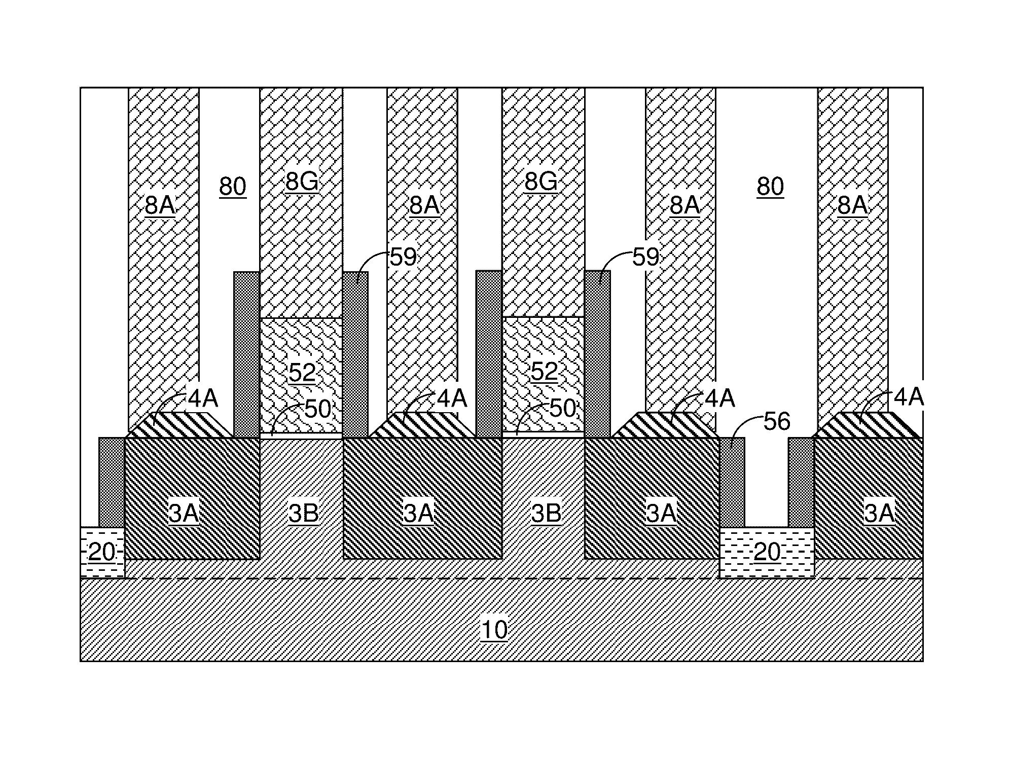
[0069]As stated above, the present disclosure relates to a method of preventing merger of raised active regions from adjacent semiconductor fins employing a fin end spacer, and structures formed by the same. These aspects of the present disclosure are now described in detail with accompanying figures. It is noted that like reference numerals refer to like elements across different embodiments. The drawings are not necessarily drawn to scale. As used herein, ordinals such as “first” and “second” are employed merely to distinguish similar elements, and different ordinals may be employed to designate a same element in the specification and / or claims.

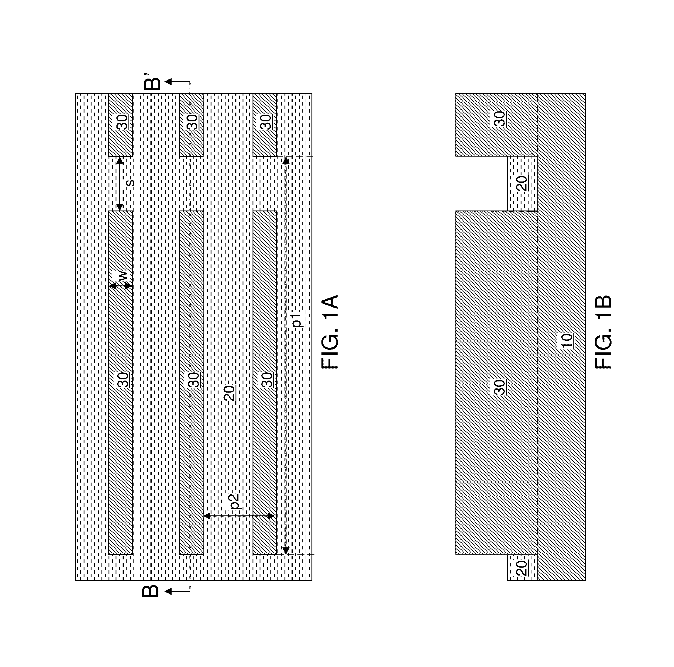
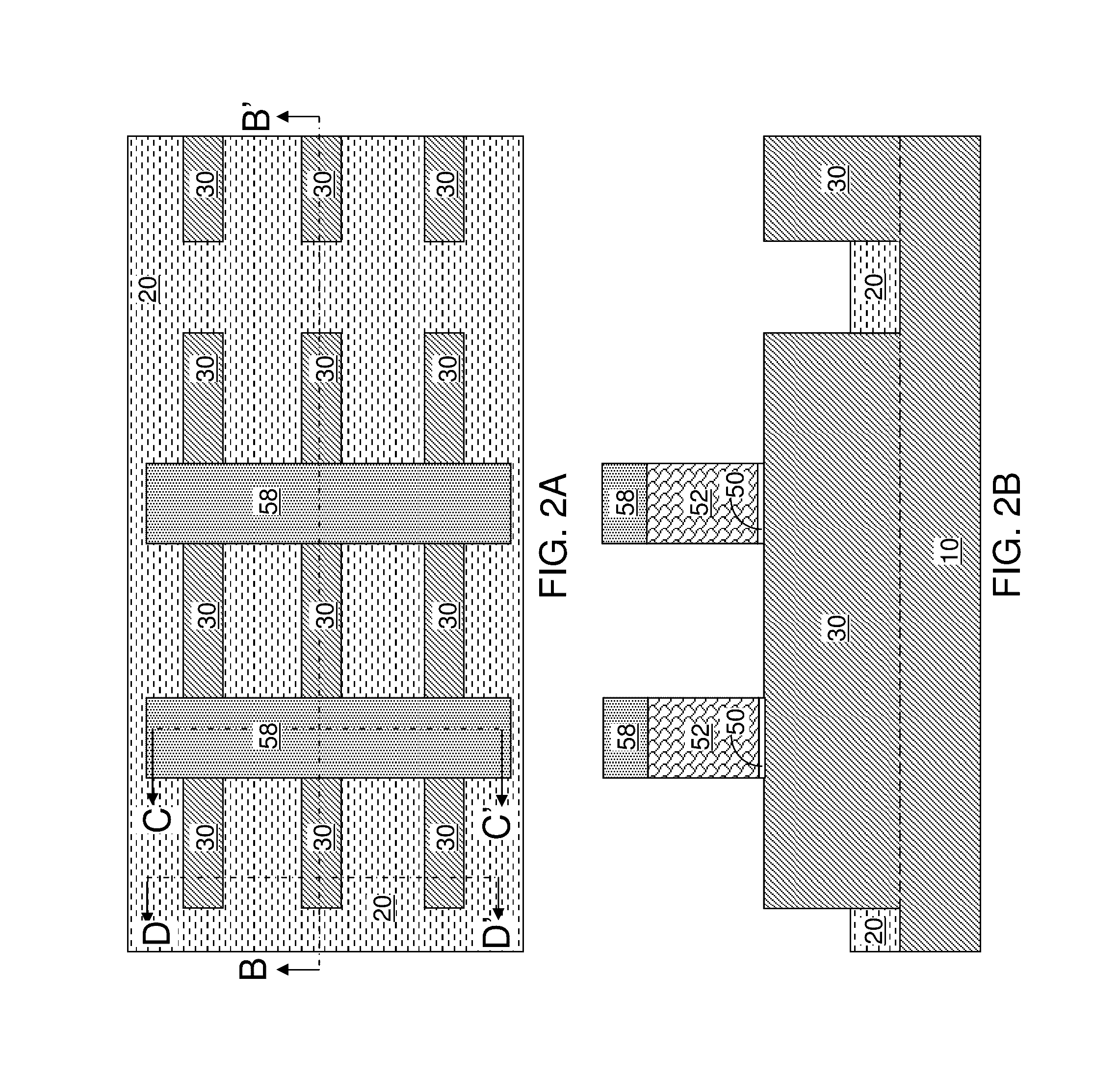
[0070]Referring to FIGS. 1A and 1B, a first exemplary semiconductor structure according to an embodiment of the present disclosure can be formed by providing a semiconductor substrate, which can be a bulk semiconductor substrate or a semiconductor-on-insulator (SOI) substrate. At least an upper portion of the semiconductor substrate include...


PUM


Abstract

After formation of gate structures over semiconductor fins and prior to formation of raised active regions, a directional ion beam is employed to form a dielectric material portion on end walls of semiconductor fins that are perpendicular to the lengthwise direction of the semiconductor fins. The angle of the directional ion beam is selected to be with a vertical plane including the lengthwise direction of the semiconductor fins, thereby avoiding formation of the dielectric material portion on lengthwise sidewalls of the semiconductor fins. Selective epitaxy of semiconductor material is performed to grow raised active regions from sidewall surfaces of the semiconductor fins. Optionally, horizontal portions of the dielectric material portion may be removed prior to the selective epitaxy process. Further, the dielectric material portion may optionally be removed after the selective epitaxy process.

Description

BACKGROUND[0001]The present disclosure relates to a semiconductor structure, and particularly to a method of preventing merger of raised active regions from adjacent semiconductor fins employing a fin end spacer, and structures formed by the same.[0002]Fin field effect transistors are widely employed in advanced semiconductor circuits for their superior performance over planar field effect transistors. Fin field effect transistors provide a high on-current per area and full depletion of a channel during operation. One of the challenges for implementing fin field effect transistors is the tendency for raised active regions, which include raised source regions and raised drain regions, in adjacent semiconductor fins to be electrically shorted unless sufficient lateral distance is provided among the adjacent semiconductor fins. While an electrical short between two semiconductor fins may be avoided by increasing a lateral spacing between the two semiconductor fins, the increase in late...

Claims


Application Information

Patent Timeline
IPC IPC(8): H01L27/088H01L29/78H01L21/02H01L21/265H01L21/311H01L21/762H01L29/06H01L29/08H01L29/417H01L29/66
CPCH01L29/66795H01L21/0217H01L21/02164H01L21/02238H01L21/02247H01L21/02252H01L21/02274H01L21/26566H01L21/31111H01L21/762H01L29/0653H01L29/0847H01L29/41783H01L29/41791H01L29/785H01L29/7848H01L21/26533H01L21/26586H01L21/823412H01L21/823418H01L21/823431H01L21/823481H01L21/845
Inventor ALPTEKIN, EMREJAIN, SAMEER H.SARDESAI, VIRAJ Y.TRAN, CUNG D.VEGA, REINALDO A.
Owner TESSERA INC
Why Eureka
Try Eureka