Method for forming a capacitive isolation trench and substrate comprising such a trench

Pending Publication Date: 2022-01-27
STMICROELECTRONICS CROLLES 2
View PDF0 Cites 0 Cited by
  • Summary
  • Abstract
  • Description
  • Claims
  • Application Information

AI Technical Summary

Benefits of technology

The patent text describes a method that prevents a cavity from forming in a safety trench during manufacturing. The technical effect of this patent is to improve the reliability and performance of semiconductor devices.

Problems solved by technology

Thus, the trench obtained at the end of this method is full and does not contain any cavity capable of accumulating undesirable materials, unlike the trenches of the prior art.

Method used


Image

  • Method for forming a capacitive isolation trench and substrate comprising such a trench
  • Method for forming a capacitive isolation trench and substrate comprising such a trench
  • Method for forming a capacitive isolation trench and substrate comprising such a trench

Examples


Embodiment Construction

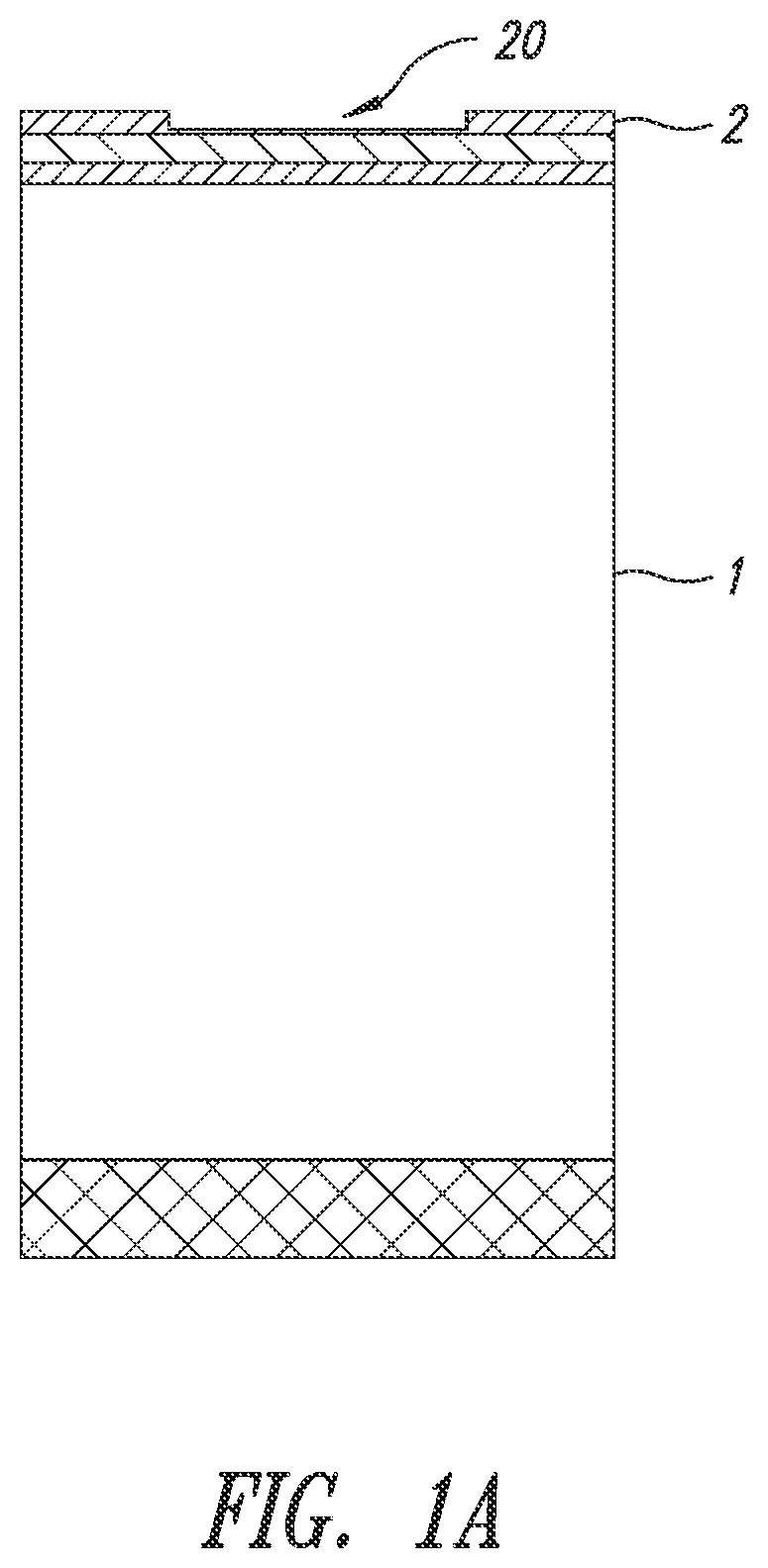
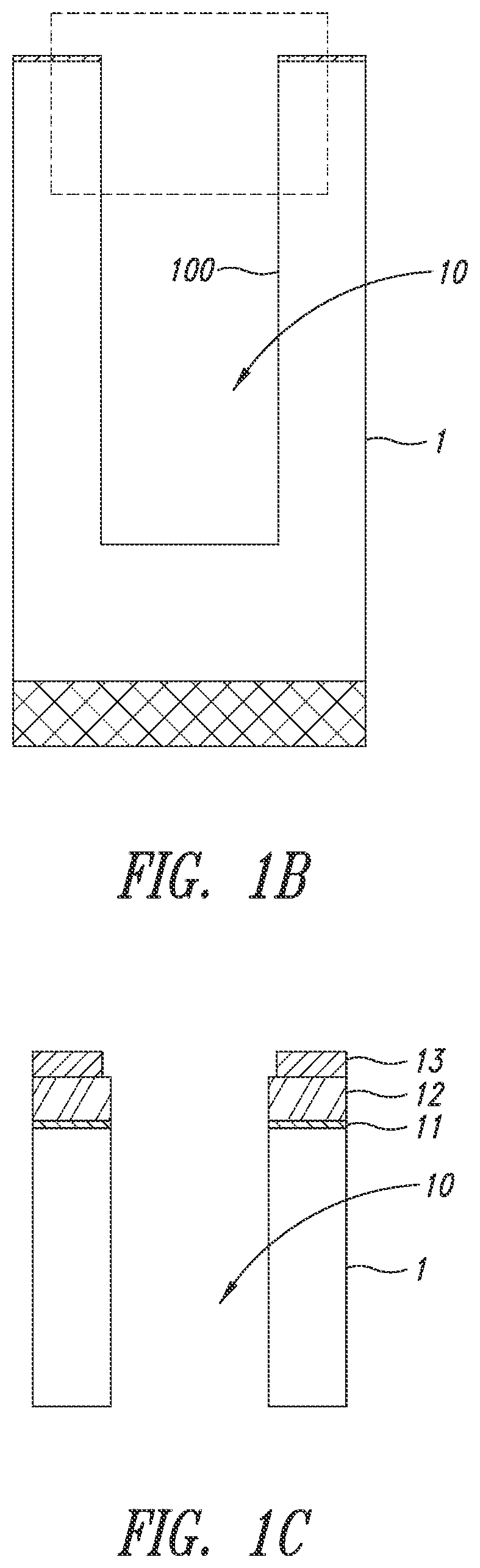
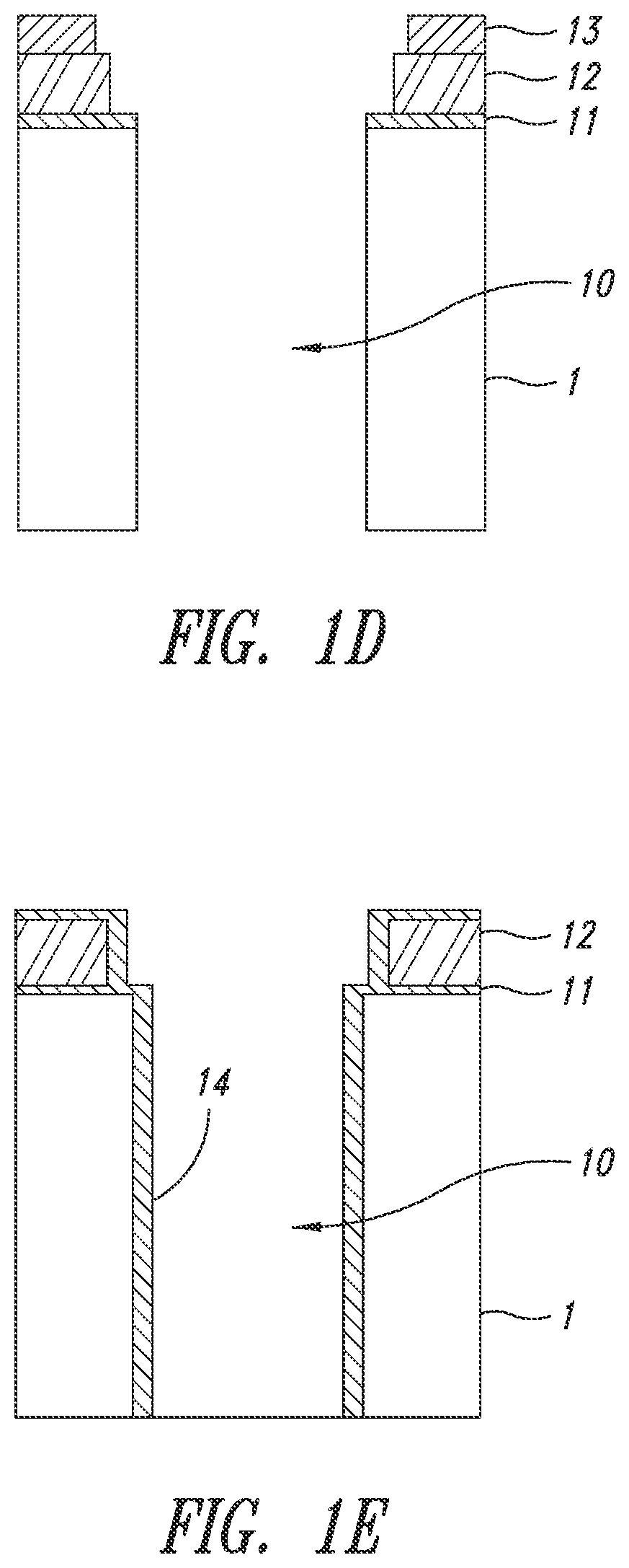
[0052]A capacitive isolation trench can be formed according to the method described with reference to FIGS. 1A to 1I.

[0053]As illustrated in FIG. 1A, a mask 2 is formed on a semiconductor substrate 1 by photolithography. Said mask comprises at least one opening 20 delimiting, on the surface of the substrate 1, the section of a trench to be formed in said substrate.

[0054]With reference to FIGS. 1B and 1C, a trench 10 is formed in the thickness of the substrate 1 from the surface exposed by the opening 20 of the mask.

[0055]With reference to FIG. 1D, a partial pull back of the stack of layers which covers the substrate 1 is implemented. Said pull back can be carried out in particular by selective etching of the layers 12 and 13 in a direction parallel to the main surface of the substrate 1, on either side of the trench 10.

[0056]With reference to FIG. 1E, a deposition of a silicon oxide (SiO2) layer 14 is implemented in the trench. This deposition is substantially conformal, so that the...


PUM


Abstract

A method for forming a capacitive isolation trench in a semiconductor substrate includes digging a trench from a main surface of the substrate, the trench including an upper portion gradually widening from a neck in the direction of a lower portion of the trench. A coating of a first electrically isolating material is formed on the walls of the trench. A first semiconductor material is deposited on the coating, with the deposition being interrupted so as to leave a free space between the walls of the trench, the free space having an opening at the neck. A second electrically isolating material is deposited in the trench, with the deposition resulting in the formation of a plug closing the opening to form a closed cavity. The plug is etched so as to open the cavity, and a second semiconductor material or a metal is deposited so as to fill the cavity.

Description

CROSS-REFERENCE TO RELATED APPLICATION[0001]This application claims the priority benefit of French patent application number FR2007905, filed on 27 Jul. 2020, which is hereby incorporated by reference to the maximum extent allowable by law.BACKGROUNDTechnical Field[0002]The present disclosure relates to a method for forming a capacitive isolation trench in a semiconductor substrate. This method can in particular be implemented during the manufacture of semiconductor substrates for image sensors, said capacitive isolation trench being intended to electrically isolate two adjacent pixels.Description of the Related Art[0003]Capacitive Isolation Trenches, known by the acronym CDTI (from the term “Capacitive Deep Trench Isolation”) are used for rear-illuminated image sensors. Such sensors are formed from a semiconductor substrate, in particular a silicon substrate, wherein a plurality of photodiodes each defining a pixel of the sensor are arranged. Capacitive isolation trenches are arran...

Claims


Application Information

Patent Timeline
IPC IPC(8): H01L21/762H01L27/146H01L21/02
CPCH01L21/76224H01L21/763H01L21/02271H01L27/1463H01L21/3065H01L21/76229
Inventor MONNIER, DENISLEVERD, FRANCOIS
Owner STMICROELECTRONICS CROLLES 2
Why Eureka
Try Eureka