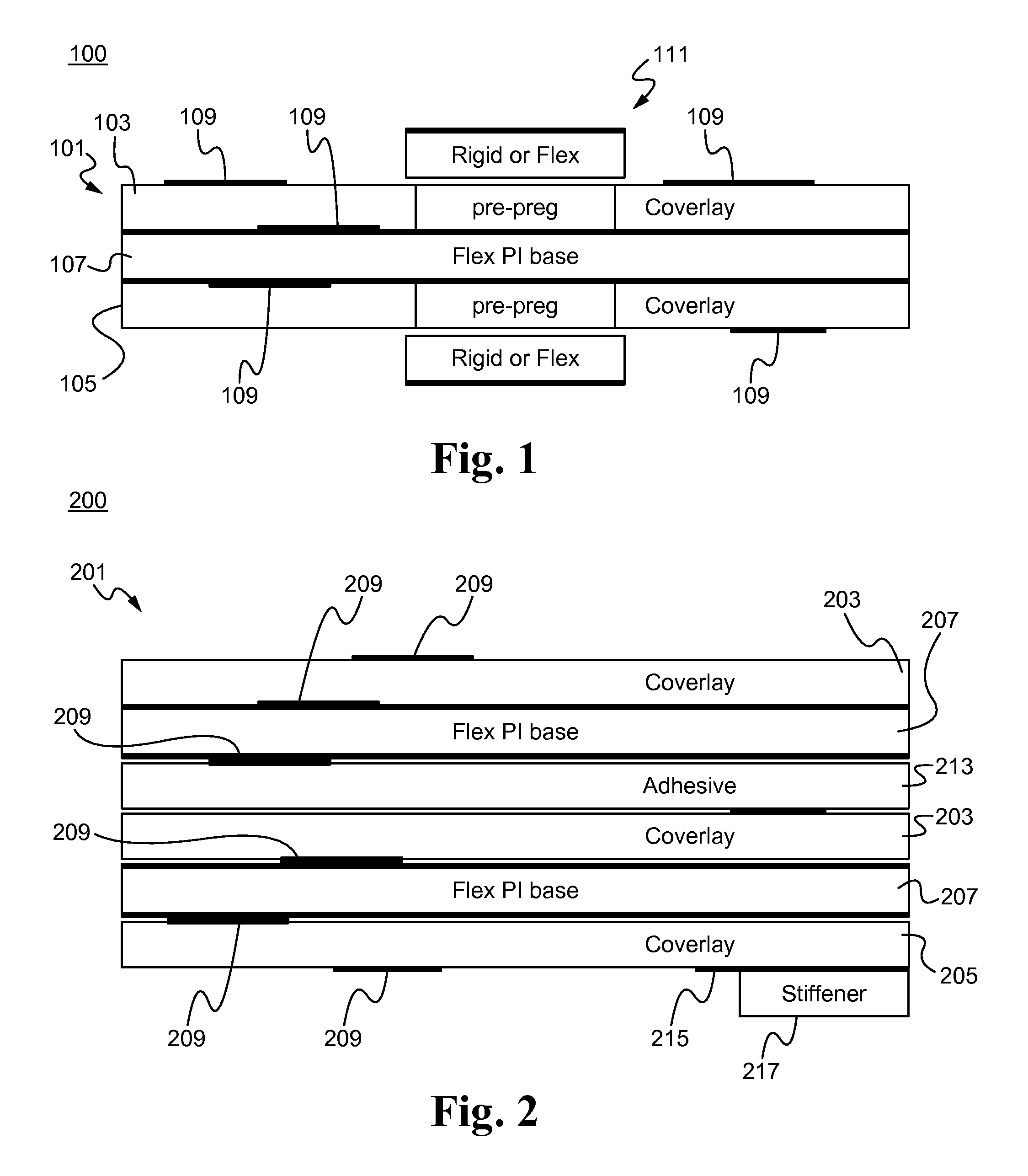
[0004]Mechanical measures strengthen a flexible circuit board or deformable electronic by manipulating the location and / or intensity of the stress concentration or to limit bending, torsion, and stretching. A material layer is patterned onto the flexible circuit board with a specific pattern and place of deposition in order to modify the stress concentration and profile of the circuit board and increase its overall strength. The material layer may be configured to modify the stress concentrations during bending away from the weak points in the assembly or to spread the stress during bending by increasing the radius of the bend curvature and therefore decreasing the chance of mechanical failure. Particularly, the mechanical measures can be used in order to strengthen and extend the life of wearable electronics as well as for in vivo and in vitro applications with wearable medical electronic devices. Additionally, the printed circuit board can be configured having a multi-layer body, one or more layers of which comprise a rigid component section and one or more layers of which comprise a flexible section including one or more coverlays comprising a polymer based film and attached throughout the circuit board for insulation and added flexibility.
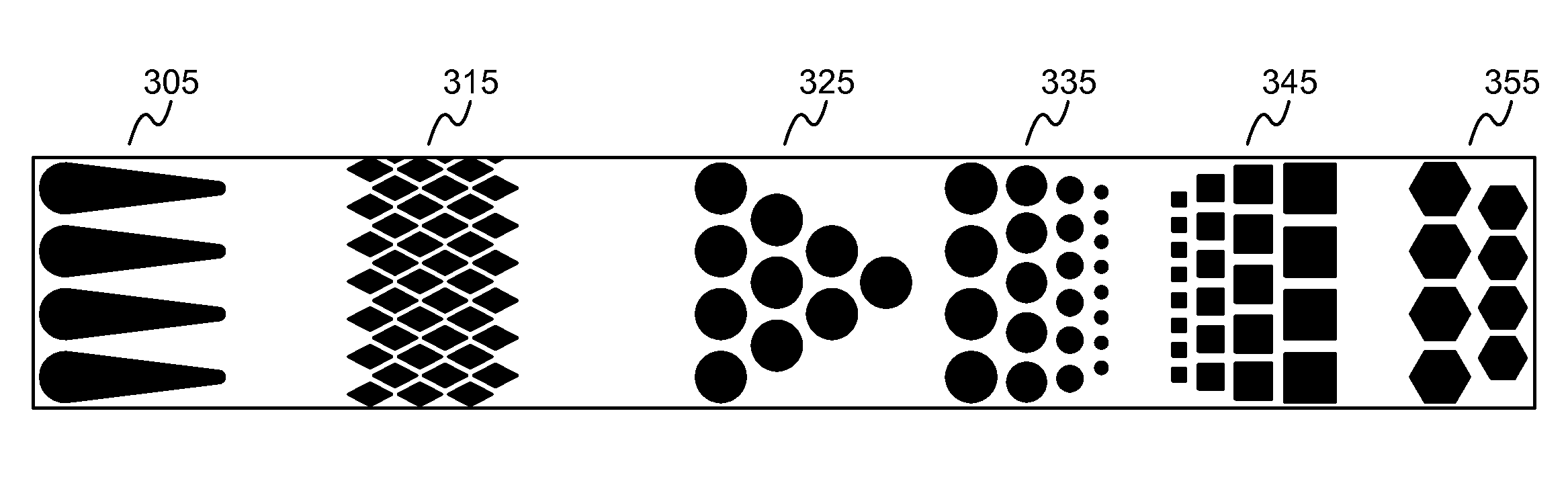
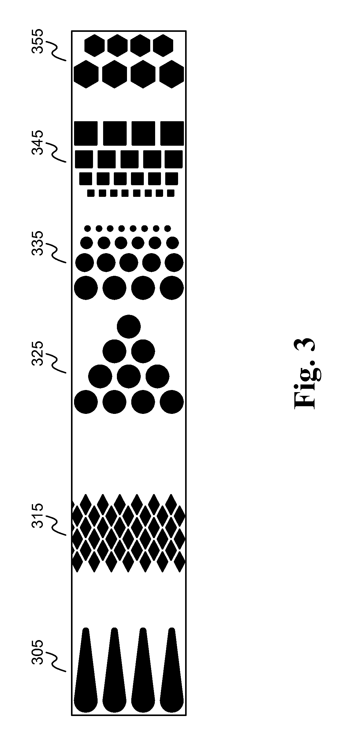
[0005]In one aspect, a deformable electronic body comprising a flexible base with one or more rigid component layers and one or flexible component layers coupled to the flexible base and a material layer deposited on the body with a specific material pattern and attached at a specific location on the body in order to modify the stress concentration of the deformable electronic and increase its overall strength. In some embodiments, the pattern of the material layer and the placement of the material layer modifies the stress concentration away from the weak points of the deformable electronic. Alternatively or in combination, the pattern of the material layer and the deposition placement of the material layer increases a radius of a curvature of the deformable electronic and decreases its chance of mechanical failure. The material layer is able to be patterned and deposited on a flexible portion of the deformable electronic and comprises an effective stiffness that decreases with distance from a rigid portion of the deformable electronic. The material layer is able to comprise a high elastic modulus. In some embodiments, the material layer comprises one or a combination of metal, polymer, cloth glass weave, polymers, and natural fibers. In some embodiments, the pattern comprises one or a combination of interlocking cones, rhomboids, circles, hexagons, and squares. The material layer is able to be photo-patterned, die-cut, laser-cut, silk-screened, and injection molded. Particularly, the strength of the deformable electronic is increased in a X dimension, a Y dimension, a Z dimension, and other dimension. In some embodiments, the material layer is attached inside or outside of the deformable electronic by bonding or lamination, or to the casing by bonding. In some embodiments, the material layer is attached to a rigid, a rigid-flex, a stretch, a rigid-stretch, or a mechanism housing of the deformable electronic. In some embodiments, the deformable electronic comprises a flexible circuit board.
[0006]In another aspect, a method of strengthening a deformable electronic comprises patterning a material layer into a specific pattern based upon one or more characteristic of the deformable electronic and depositing the material layer onto the deformable electronic, wherein the pattern of the material layer and the deposition placement of the material layer modifies the stress concentration of the deformable electronic in order to increase its overall strength. In some embodiments, the pattern of the material layer and the deposition placement of the material layer modifies the stress concentration away from the weak points of the deformable electronic. Alternatively or in combination, the pattern of the material layer and the deposition placement of the material layer increases a radius of a curvature of the deformable electronic and decreases its chance of mechanical failure. The material layer is able to be patterned and deposited on a flexible portion of the deformable electronic and comprises an effective stiffness that decreases with distance from a rigid portion of the deformable electronic. The material layer is able to comprise a high elastic modulus. In some embodiments, the material layer comprises one or a combination of metal, polymer, cloth glass weave, polymers, and natural fibers. In some embodiments, the pattern comprises one or a combination of interlocking cones, rhomboids, circles, hexagons, and squares. The material layer is able to be photo-patterned, die-cut, laser-cut, silk-screened, and injection molded. Particularly, the strength of the deformable electronic is increased in a X dimension, a Y dimension, a Z dimension, and other dimension. In some embodiments, the material layer is attached inside or outside of the deformable electronic by bonding or lamination, or to the casing by bonding. In some embodiments, the material layer is attached to a rigid, a rigid-flex, a stretch, a rigid-stretch, or a mechanism housing of the deformable electronic. In some embodiments, the deformable electronic comprises a flexible circuit board.
