Method of manufacturing module

a manufacturing method and module technology, applied in the direction of sustainable manufacturing/processing, final product manufacturing, printed circuit non-printed electric components association, etc., can solve the problems of increased manufacturing cost of the module, difficulty in adjusting the output power of a laser, and variations in the accuracy with which the via hole is formed, so as to reduce cost and manufacturing time, and increase the density of electronic components mounted in the module

Active Publication Date: 2017-01-03
MURATA MFG CO LTD
View PDF25 Cites 0 Cited by
  • Summary
  • Abstract
  • Description
  • Claims
  • Application Information

AI Technical Summary

Benefits of technology

[0006]However, in the invention disclosed in Patent Document 1, the via conductors 506 are formed in such a manner that via holes formed by a laser process in the resin layers 503 provided in the wiring substrate 501 are, after desmearing processing, filled with conductor paste including, for example, Ag and Cu, or subjected to via fill plating processing. When the via holes are formed in the resin layers 503 by a laser process in this manner, it is difficult to adjust the output power of a laser, resulting in a problem in that there are variations in the accuracy with which the via holes are formed. Further, since the via conductors 506 are formed in the resin layers 503 through a plurality of process steps, the manufacturing cost of the module is increased and it is difficult to reduce the time required to manufacture the module. In addition, there is a problem in that a chemical solution used when via holes formed in the resin layers 503 by a laser process are subjected to desmearing processing or a chemical solution used for via fill plating processing erodes the resin layers 503 and the wiring substrate 501.
[0007]In view of the above-described problems, it is an object of the present invention to provide a low-cost module which enables interlayer connection without providing via holes and which can be manufactured in a short time.

Problems solved by technology

When the via holes are formed in the resin layers 503 by a laser process in this manner, it is difficult to adjust the output power of a laser, resulting in a problem in that there are variations in the accuracy with which the via holes are formed.
Further, since the via conductors 506 are formed in the resin layers 503 through a plurality of process steps, the manufacturing cost of the module is increased and it is difficult to reduce the time required to manufacture the module.
In addition, there is a problem in that a chemical solution used when via holes formed in the resin layers 503 by a laser process are subjected to desmearing processing or a chemical solution used for via fill plating processing erodes the resin layers 503 and the wiring substrate 501.

Method used


Image

  • Method of manufacturing module
  • Method of manufacturing module
  • Method of manufacturing module

Examples


first embodiment

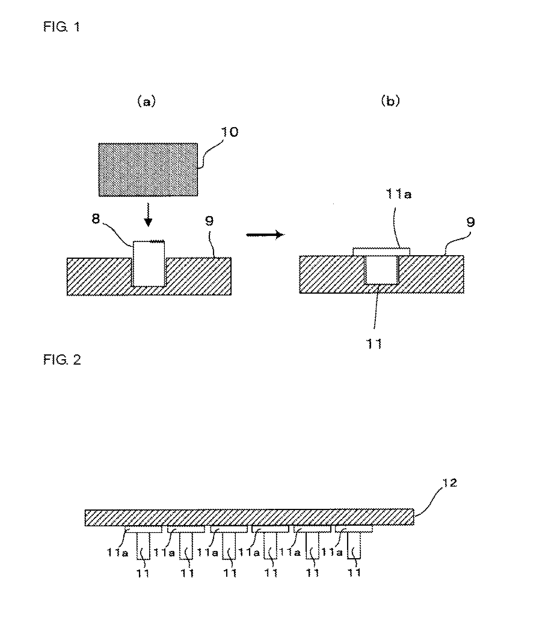
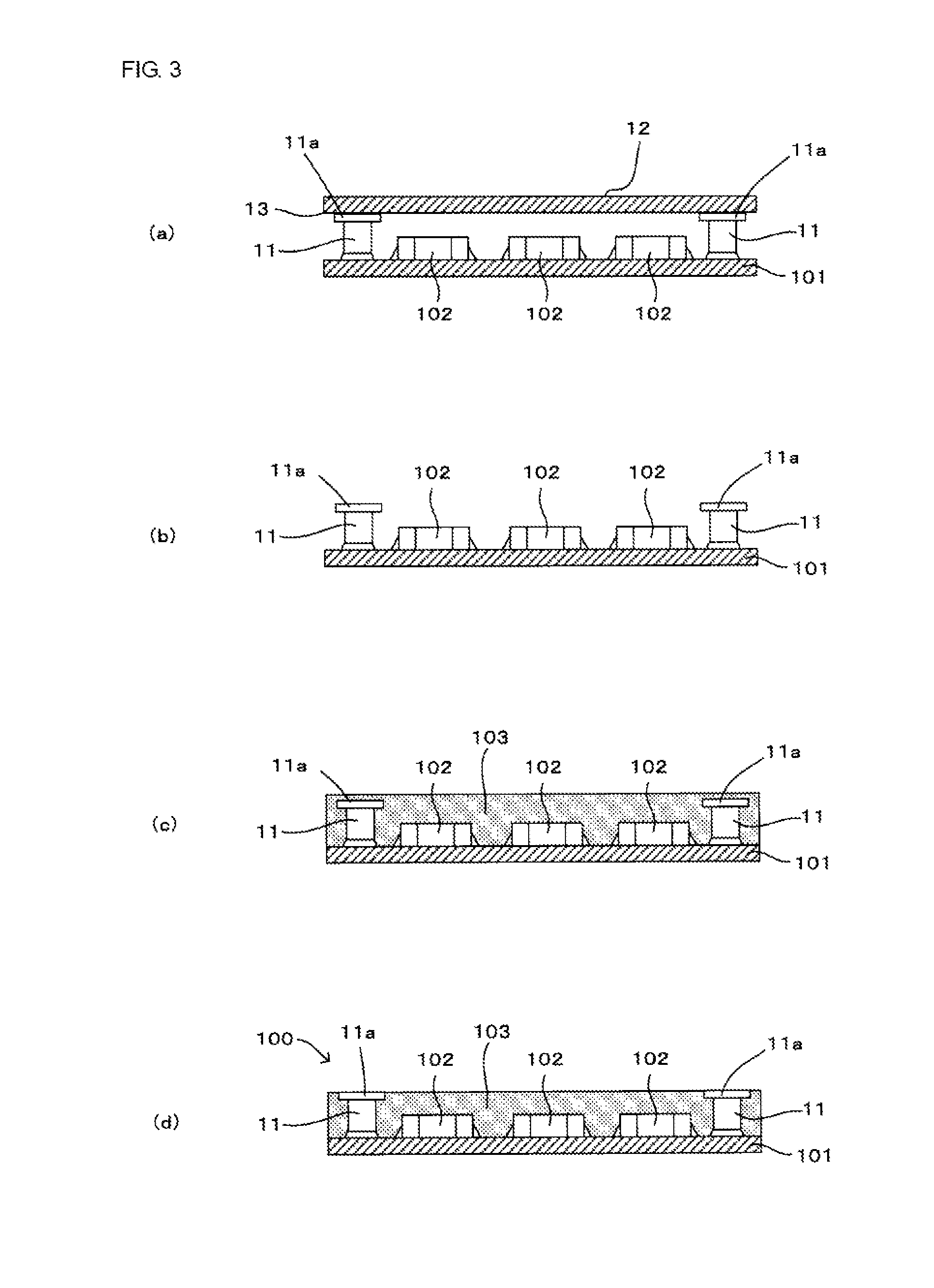
[0041]A module according to a first embodiment of the present invention will be described with reference to FIG. 1 to FIG. 4. FIG. 1 is a diagram illustrating a method of manufacturing the connection terminals used in a module according to the first embodiment, FIG. 2 is a diagram illustrating the connection terminals, and FIG. 3 is a diagram illustrating a method of manufacturing the module according to the first embodiment, where (a) to (d) respectively illustrate different steps. FIG. 4 is a diagram illustrating an example of the arrangement of electronic components.

[0042]The method of manufacturing a module described in the present embodiment is used for manufacturing high-frequency circuit modules mounted, for example, on the mother boards of communication mobile terminals, such as various communication modules including a Bluetooth (registered trade mark) module and a wireless LAN module, an antenna switch module, and a power supply module.

(Method of Manufacturing Modules)

[004...

second embodiment

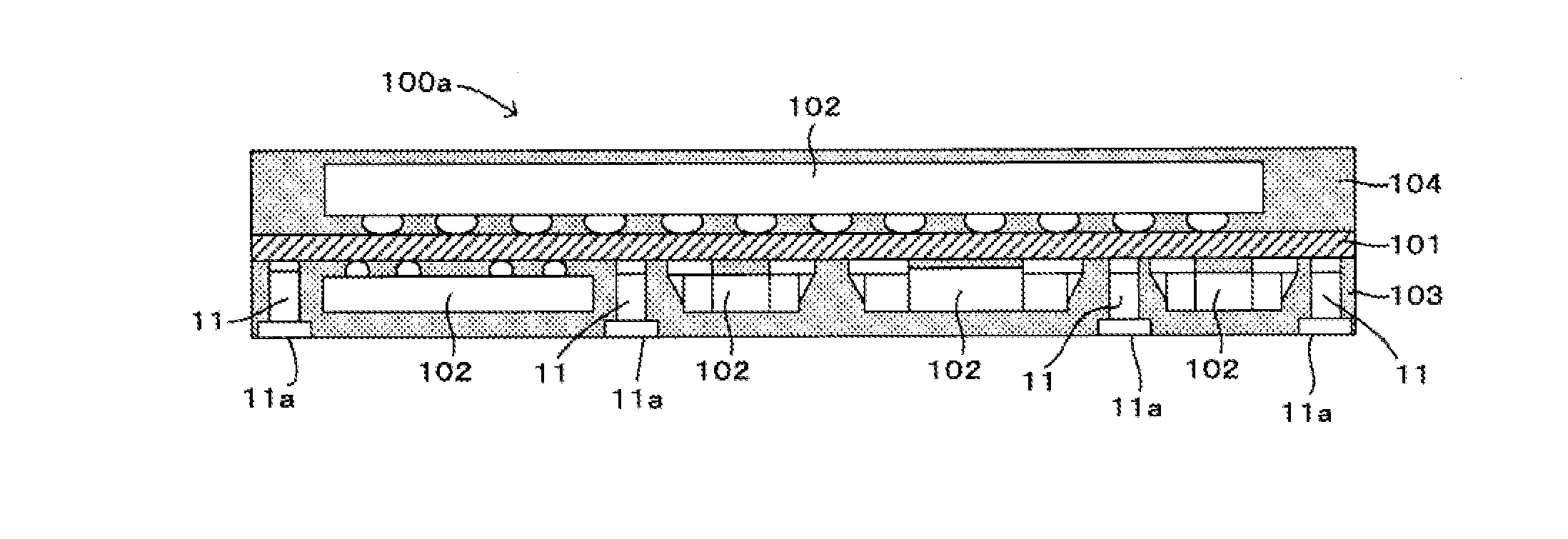
[0073]A module 100a according to a second embodiment of the present invention will be described with reference to FIG. 5. FIG. 5 is a diagram illustrating the module 100a according to the second embodiment of the present invention.

[0074]Unlike the first embodiment described above, in the module 100a of the present embodiment, the electronic components 102 are further mounted on the other main surface of the wiring substrate 101 of the module 100a (the second mounting step), and these electronic components 102 are sealed with a second resin layer 104 (the second sealing step), as illustrated in FIG. 5. The rest of the configuration is the same as that of the above-mentioned first embodiment and the description thereof is omitted by attaching the same reference symbols to components common in the embodiments.

[0075]Accordingly, this configuration is practical since the density of the electronic components 102 mounted in the module 100a can be increased, as a result of the electronic co...

third embodiment

[0076]A module 100b according to a third embodiment of the present invention will be described with reference to FIG. 6. FIG. 6 is a diagram illustrating the module 100b according to the third embodiment of the present invention.

[0077]Unlike the second embodiment described above, in the module 100b according to the present embodiment, a metal shield layer 105 is provided on the second resin layer 104 which is provided on the other main surface of the wiring substrate 101 of the module 100b, as illustrated in FIG. 6. The rest of the configuration is the same as that of the first and second embodiments and the description thereof is omitted by attaching the same reference symbols to components common in the embodiments. Note that it is preferable that the metal shield layer 105 be electrically connected to GND wiring provided at the wiring substrate 101.

[0078]With this configuration, since the metal shield layer 105 is provided on the second resin layer 104, in particular, noise is in...


PUM

PropertyMeasurementUnit
diameteraaaaaaaaaa
output poweraaaaaaaaaa
magnetic forceaaaaaaaaaa

Abstract

When forming a module 100 having a configuration in which a column-shaped connection terminal 11, which forms an interlayer connection conductor, and an electronic component 102 are mounted on a wiring substrate 101 and sealed with a resin, the column-shaped connection terminal 11 which has a substantially T-shaped cross section and in which a first end portion has a larger diameter than a second end portion is prepared (the preparation step), an electronic component 102 is mounted on one main surface of the wiring substrate 101 and the connection terminal 11 is mounted on the one main surface in such a manner that the second end portion of the connection terminal 11 having a smaller diameter is connected to the wiring substrate 101 (the mounting step), and the electronic component 102 and the connection terminal 11 are sealed with a resin layer 103 (the sealing step).

Description

BACKGROUND OF THE INVENTION[0001]1. Field of the Invention[0002]The present invention relates to methods of manufacturing a module that includes a plurality of connection terminals forming interlayer connection conductors and relates to the module.[0003]2. Description of the Related Art[0004]To date, as shown by an example module illustrated in FIG. 8, a module 500 is known in which various electronic components 502 mounted on both surfaces of a wiring substrate 501 are sealed with resin layers 503 (for example, refer to Patent Document 1). In this case, a metal shield layer 504 is provided on one main surface of the module 500, and mounting electrodes 505 for external connection are provided on the other main surface. The metal shield layer 504 and the mounting electrodes 505 are electrically connected to the wiring layer of the wiring substrate 501 through respective via conductors 506 for interlayer connection.[0005]Patent Document 1: International Publication No. 2005 / 078796 (pa...

Claims


Application Information

Patent Timeline
Patent Type & Authority Patents(United States)
IPC IPC(8): H05K3/30H01L23/498H01L23/31H05K1/11H01L21/48H05K3/40H01L23/552H01L25/065H05K3/46H01L23/538H05K3/28H05K1/18
CPCH05K1/11H01L21/4853H01L23/3121H01L23/49811H01L23/5389H01L23/552H01L25/0652H05K3/303H05K3/4015H05K3/4046H05K3/4644H01L25/0655H01L2224/16225H01L2924/1531H01L2924/19105H01L2924/19106H05K1/181H05K3/284H05K2201/0715H05K2201/1031H05K2201/10242H05K2201/10515H05K2203/1316Y02P70/611Y10T29/49146Y02P70/50
Inventor OGAWA, NOBUAKIOTSUBO, YOSHIHITO
Owner MURATA MFG CO LTD
Why Eureka
Try Eureka