[0017]In order to overcome the above-described drawbacks previously associated with the provision of a bonding layer between a base member and an electrostatic chuck (ESC), heated electrostatic chuck or semiconductor wafer heater attached thereto, the present invention implements a plasma deposition technique, also referred to herein as plasma spraying, to deposit at least the thermal barrier coating (TBC) layer, but more preferably, to deposit each of the layers in the structure formed directly on the base layer. This eliminates the need for problematic bonding agents / layers which can degrade and negatively affect the thermal uniformity and processing conditions, or brazing agents which affect the thermal transfer properties and cause heat loss, as discussed above. This also greatly simplifies the overall formation process by using a single technique, rather than requiring different machinery and processes for forming multiple layers, which in turn reduces costs and improves production efficiency.
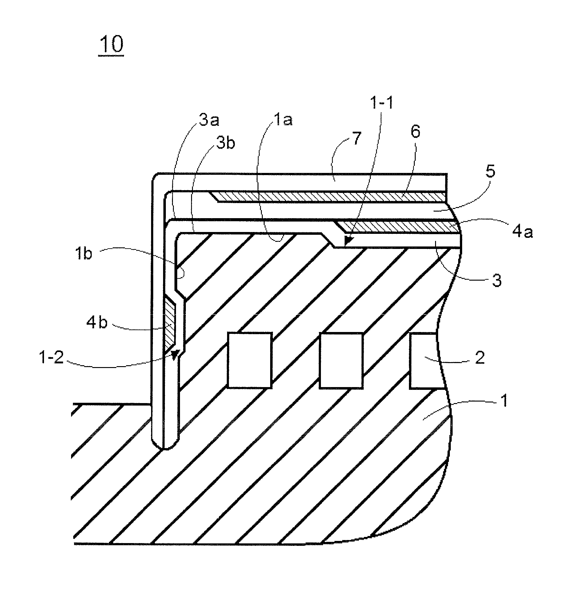
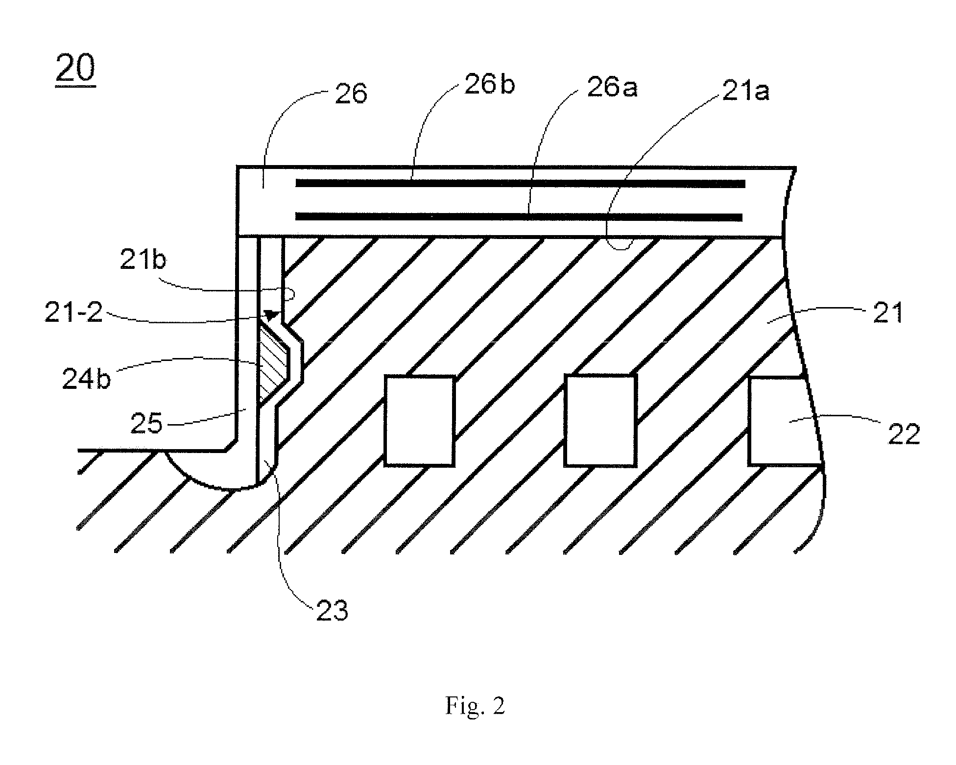
[0019]In addition, thermal mismatching is further reduced by controlling the porosity of the TBC layer. More specifically, because the base material, such as aluminum, for example, has a high CTE, a portion of the TBC layer directly adjacent the base should have a relatively high porosity to overcome the CTE mismatching issue. Since the CTE changes with porosity in plasma spray deposition, a lower porosity will yield a lower CTE, and a higher porosity will result in a higher CTE. As the distance from the interface between the base and the TBC layer increases, the porosity of the TBC layer should be reduced in order to better match up with the CTE of the insulating layer that is deposited thereon, such as an alumina insulating layer, for example. The provision of a graded thermal barrier coating (GTBC) layer in this manner therefore overcomes significant drawbacks associated with the prior art by reducing thermal conductivity, thermal mismatching and preventing bowing to ensure better thermal uniformity and improved performance characteristics.
[0020]In order to control the thickness of the heating element and ensure overall thermal uniformity, one or more heating elements according to the present invention are patterned by machining the top and / or peripheral side surfaces of the base material to define a circuitous recessed pattern, such as a coil, zigzag, spiral, whirl or sinuous pattern, for example. The gap between adjacent heating element portions on a given surface (top or side) of the base is precisely controlled in one aspect by the process of machining the pattern recess to define a predetermined distance for maintaining thermal uniformity. The GTBC layer is then deposited by plasma spraying on the patterned base material so as to fill the valleys of the pattern (i.e., the recess) and cover the plateau peaks (gaps between the valleys) defined by the pattern shape, and then the material for the heating element is deposited thereon, also preferably by plasma spraying. The ultimate pattern of the heating element is revealed by precisely grinding the surface thereof to a predetermined thickness in order to expose the GTBC layer-covered peaks of the pattern, so that the heating element is located in a position corresponding to the pattern recess valleys, and adjacent portions thereof are separated from one another via gaps comprising the exposed peaks of the GTBC layer in locations corresponding to the plateau peaks of the pattern. This grinding process makes it possible to provide a uniform thickness for the heating element within a tolerance of ±0.005 mm, which further improves the thermal uniformity.
[0024]The present invention also solves the aforementioned problems associated with surface renewal in that the plasma-deposited upper surface layer (i.e., protective electrically insulating layer) of the ESC or semiconductor wafer heater can be easily partially removed by grinding, and a new layer is readily reapplied by plasma deposition to the required specifications to restore the proper dimensions.
[0027]Providing the peripheral side surface-located heating element overcomes the polymer build-up problems discussed above, and improves the performance longevity of conventional sintered devices (heaters, ESCs) provided in connection with the side-heated support according to the present invention.
[0029]The semiconductor wafer heater according to this aspect of the present invention offers the same benefits associated with the first aspect of the present invention described above, and overcomes the drawbacks of the prior art in a similar way. The structure is the same, with the exception of the subsequently formed chucking electrode and additional insulating layer in the heated ESC described above, as one skilled in the art can appreciate. The optional provision of the peripheral side-located heating element, as described in connection with the first aspect above, offers the same benefits, as well.

