Silicon-based multiplexer/demultiplexer for O-band

a technology of o-band and multiplexer, which is applied in the direction of optical waveguide light guide, instruments, optics, etc., can solve the problems that the internet and mobile applications continuously demand a huge amount of bandwidth for transferring photo, video, music, etc., and achieves high process tolerance, simple waveguide formation process, and enhanced production yield

Active Publication Date: 2018-07-31
MARVELL ASIA PTE LTD
View PDF3 Cites 5 Cited by
  • Summary
  • Abstract
  • Description
  • Claims
  • Application Information

AI Technical Summary

Benefits of technology

[0011]Many benefits of the Si-based two-wavelength Mux/Demux can be achieved with the present invention based on a silicon waveguide MMI block. As an example, using silicon material only is fully compatible with CMOS technology based on standard SOI wafer with a 200 nm Si-layer, which substantially simplifies the waveguide formation process and enhances production yield with high process tolerance. By utilizing general interference with mode excitations, the silicon waveguide MMI block can be optimized with ultra compact width-length dimensions for achieving power/wave

Problems solved by technology

But Internet and mobile applications continuously demand a huge amount of

Method used


Image

  • Silicon-based multiplexer/demultiplexer for O-band
  • Silicon-based multiplexer/demultiplexer for O-band
  • Silicon-based multiplexer/demultiplexer for O-band

Examples


Embodiment Construction

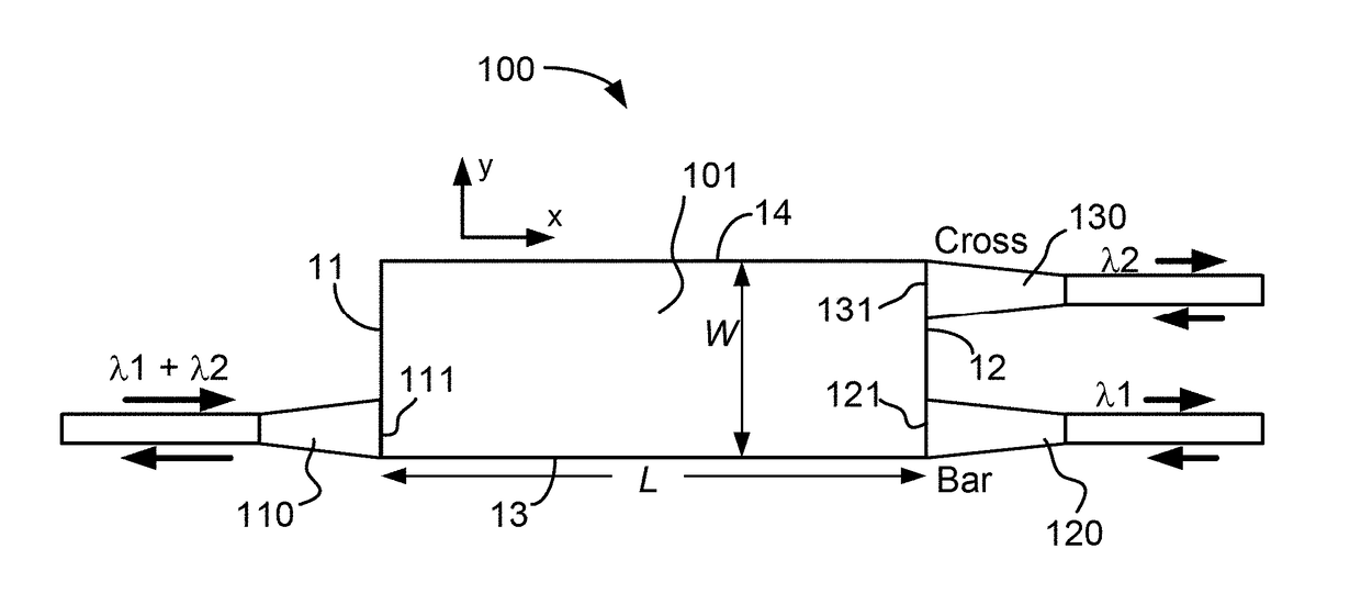
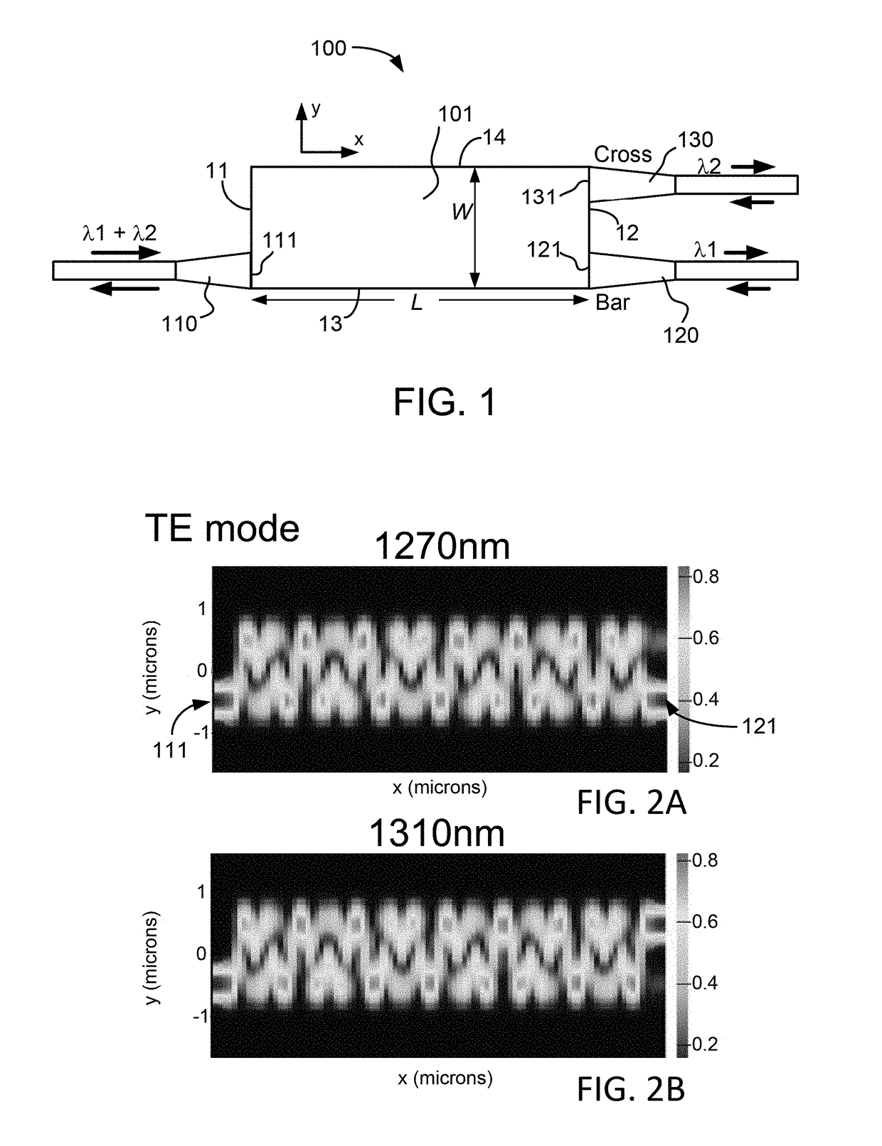
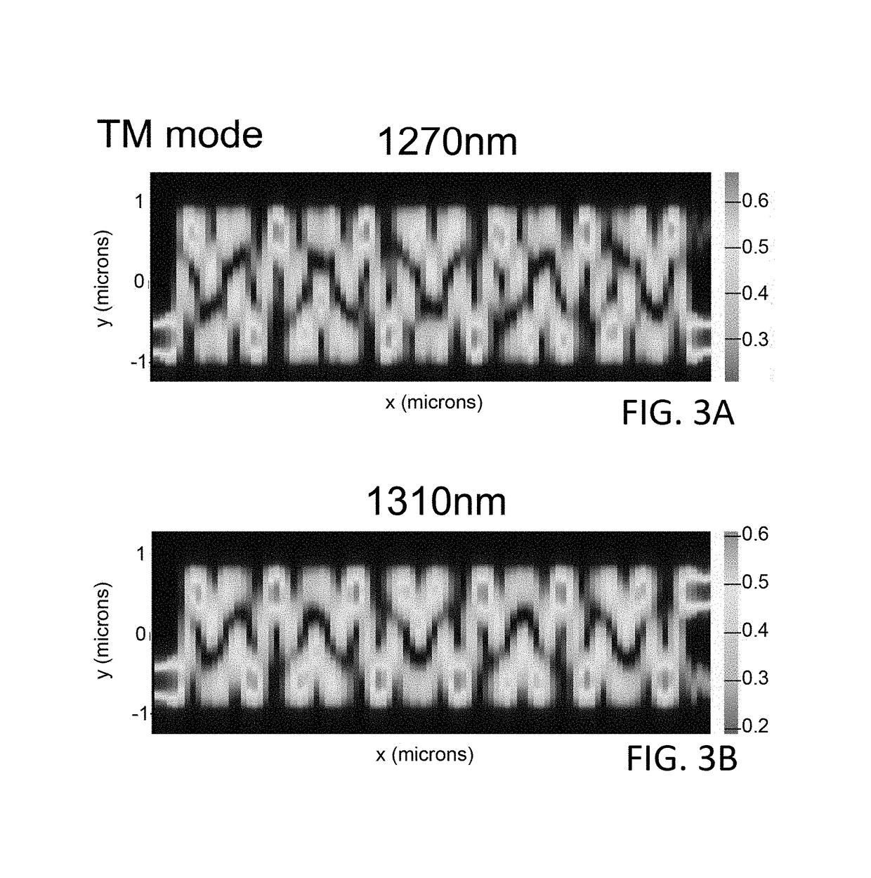
[0021]The present invention relates to photonic broadband communication device. More particularly, the present invention provides a Si-based two-wavelength Mux / Demux for O-band. Merely by example, the present invention discloses a compact multimode interference Mux / Demux based on standard 220 nm Silicon-on-Insulator (SOI) substrate with low transmission loss and high extinction ratio to combine / split to two beams of light respectively at two channel wavelengths in O-band either in Transverse Magnetic (TM) mode or Transverse Electric (TE) mode. The Si-based Mux / Demux can be integrated within a silicon photonics system in either a transmission path or reception path, though other applications are possible.

[0022]Integrated wavelength-division multiplexer (Mux) or demultiplexer (Demux) is a key element for handling expansion of optical transmission through silicon photonics circuit. It is highly desirable to design ultra-compact, simple process, and low loss Mux / Demux based on widely su...


PUM


Abstract

A multiplexer/demultiplexer for at least two wavelengths in O-band. The multiplexer/demultiplexer includes a silicon waveguide block having a first port, a second/third port respectively in bar/cross position at an opposing end plane relative to the first port. The silicon waveguide block is configured to provide a general interference excitation of a light wave of a first wavelength and a second wavelength respectively selected from two windows in O-band. The light wave is either inputted via the first port and split into a first output light of the first wavelength out of the second port and a second output light of the second wavelength out of the third port, or is combined of a first input light of the first wavelength from the second port and a second input light of the second wavelength from the third port and outputted via the first port with both wavelengths.

Description

BACKGROUND OF THE INVENTION[0001]The present invention relates to a silicon photonics device. More particularly, the present invention provides a compact Si-based MMI Mux / Demux with low loss and high extinction ratio for two wavelengths in O-band.[0002]Over the last few decades, the use of broadband communication networks exploded. In the early days Internet, popular applications were limited to emails, bulletin board, and mostly informational and text-based web page surfing, and the amount of data transferred was usually relatively small. Today, Internet and mobile applications demand a huge amount of bandwidth for transferring photo, video, music, and other multimedia files. For example, a social network like Facebook processes more than 500 TB of data daily. With such high demands on data and data transfer, existing data communication systems need to be improved to address these needs.[0003]Multiplexing has been employed to further expand the capacity of optical link. Wavelength ...

Claims


Application Information

Patent Timeline
IPC IPC(8): G02B6/12G02B6/293
CPCG02B6/29344G02B6/12007G02B6/2938G02B6/29397G02B2006/12061
Inventor LIN, JIE
Owner MARVELL ASIA PTE LTD
Why Eureka
Try Eureka