

Devices and methods with capacitive storage for latch redundancy
a capacitive storage and latch technology, applied in the field of semiconductor devices, can solve the problems of increasing the possibility of failures induced by soft errors and/or single event upset (seu), and redundancy becoming increasingly importan
- Summary
- Abstract
- Description
- Claims
- Application Information
AI Technical Summary
Benefits of technology
Problems solved by technology
Method used
Image

Examples
Embodiment Construction
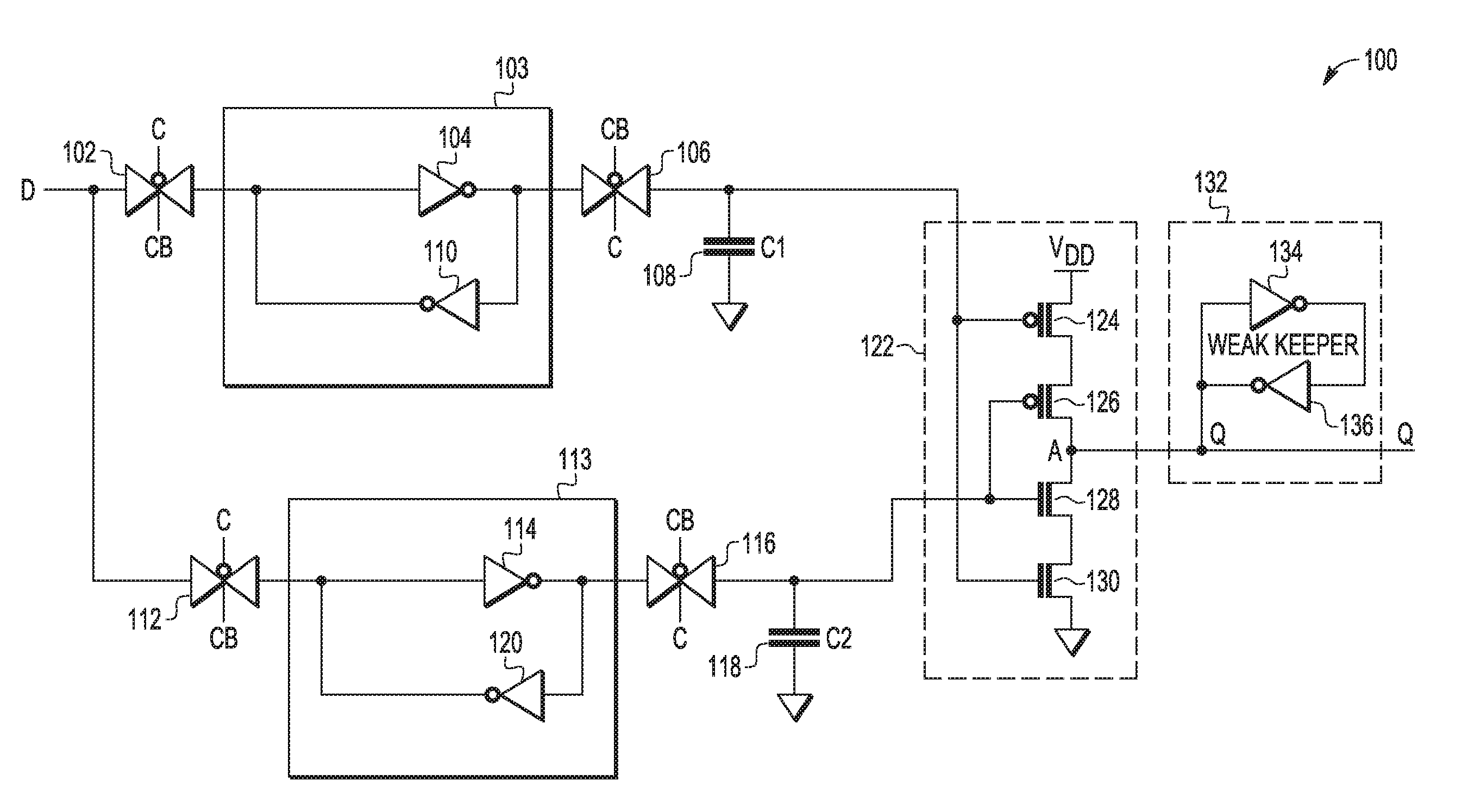
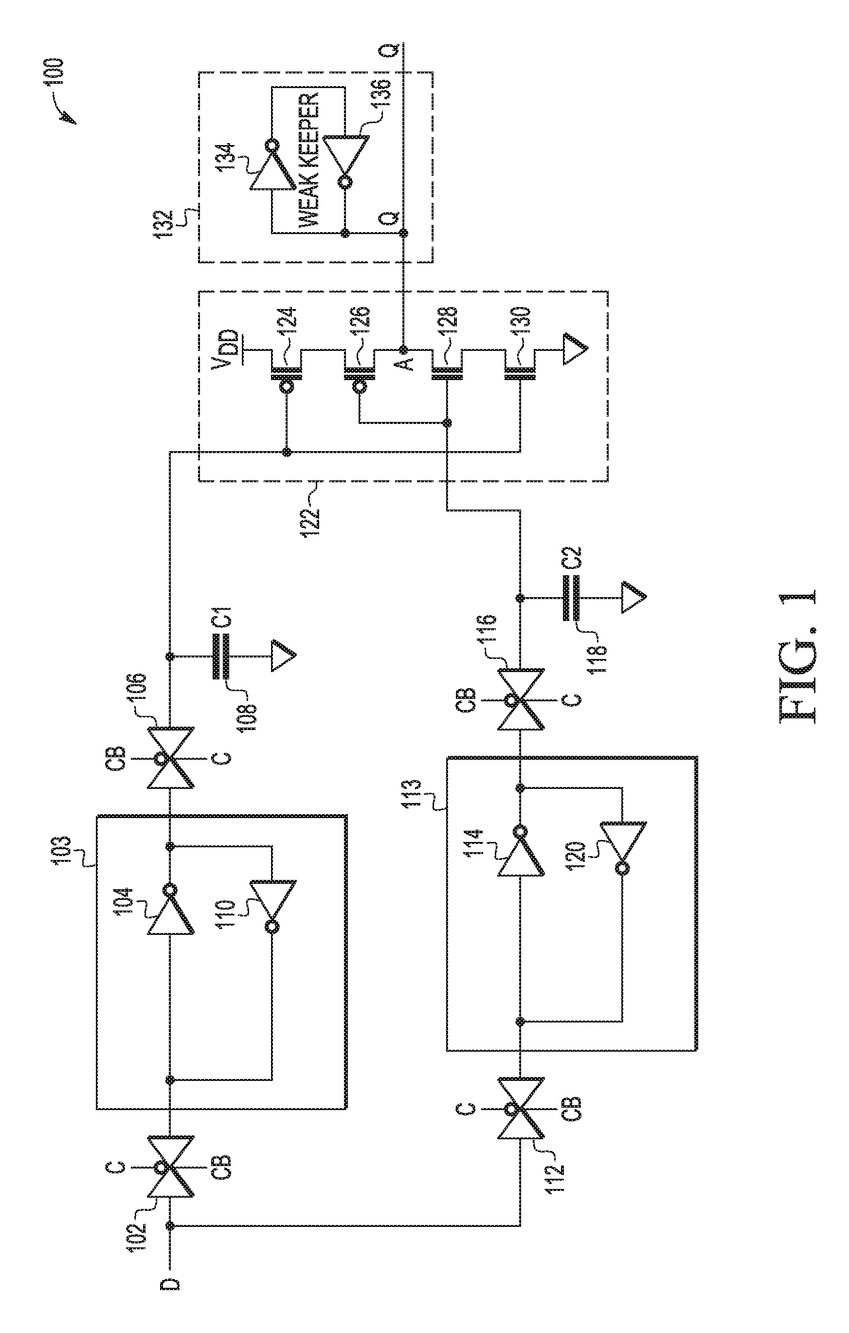
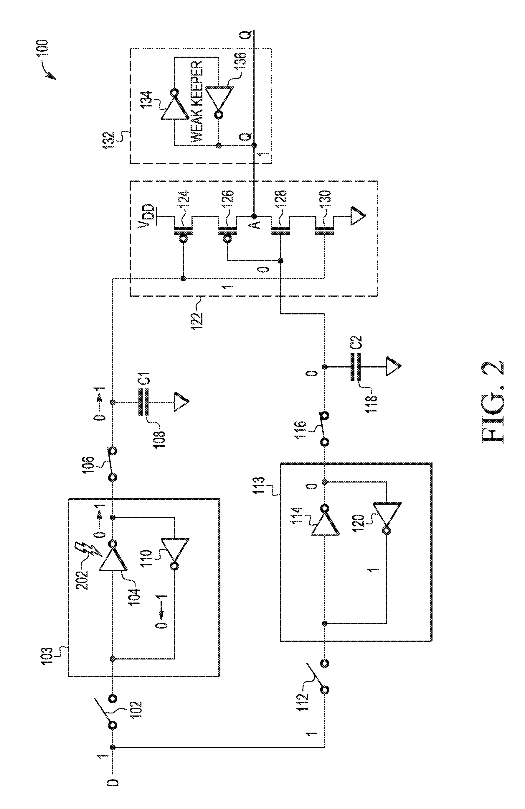
[0013]Embodiments of devices and methods disclosed herein provide master-slave latch circuits capable of outputting the original stored data even after a radiation particle strike changes the data being stored in one or the other of a master or slave latch. In some embodiments capacitors and latches are used to form a main and redundant master slave storage circuits. The outputs of the main and redundant storage elements are compared using a Muller gate. A particle strike can affect either a main storage element or a redundant storage element resulting in high-impedance state of the Muller gate. A Muller gate in a high impedance state allows a keeper circuit to maintain the original value of the stored data output thus keeping the system unaffected as before the strike. An added advantage is that area and power usage is much less than solutions that include double or triple redundancy of the latch circuits.
[0014]FIG. 1 illustrates a schematic diagram of a master-slave storage circui...
PUM
 Abstract
Description
Claims
Application Information