Method of cleaning glass substrates

a technology of glass substrate and cleaning method, which is applied in the direction of cleaning flexible articles, cleaning process and apparatus, and cleaning using liquids. it can solve the problems of rgb pixel integrity, no industry standard exists for the display glass industry for submicron particle removal, and existing cleaning process steps are not optimized to remove different defect types (organic, adhered glass or metallic)

Inactive Publication Date: 2017-02-07
CORNING INC
View PDF29 Cites 111 Cited by
  • Summary
  • Abstract
  • Description
  • Claims
  • Application Information

AI Technical Summary

Benefits of technology

[0007]Disclosed herein is a cleaning process for a glass substrate such that a pristine surface (low particle density for particles having an effective diameter greater than about 0.3 micron sizes, low levels of metallic contaminants and having improved electrostatic performance) is produced. The method is a chemically driven and mechanically assisted process using multiple cleaning solutions combined with large size LCD substrate cleaning and handling processes. The process utilizes an approach wherein particles of progressively smaller effective diameter are removed from a surface of the glass substrate by applying an in-line sequential treatment to the surface.
[0012]In an optional fourth step 130, surface treatment for better electro static discharge (ESD) characteristics of the glass substrate is performed. In this step the glass substrate is exposed to the liquid discharge of an acid solution, for example an acid solution comprising hydrofluoric acid (HF), to increase a roughness of the glass substrate surface to which the acid solution is applied.

Problems solved by technology

The same can be said for the color filter industry, as contaminants are known to adversely affect black matrix adhesion and resulting RGB pixel integrity.
Nevertheless, no industry standard exists for the display glass industry for submicron particle removal, unlike that which exists for the semiconductor industry.
In addition, existing cleaning process steps are not optimized to remove different defect types (organic, adhered glass or metallic) or varying particle size (submicron, micron or larger).

Method used


Image

  • Method of cleaning glass substrates
  • Method of cleaning glass substrates
  • Method of cleaning glass substrates

Examples


Embodiment Construction

[0035]Reference will now be made in detail to exemplary embodiments of the present disclosure, examples of which are illustrated in the accompanying drawings. Wherever possible, the same reference numbers will be used throughout the drawings to refer to the same or like parts.

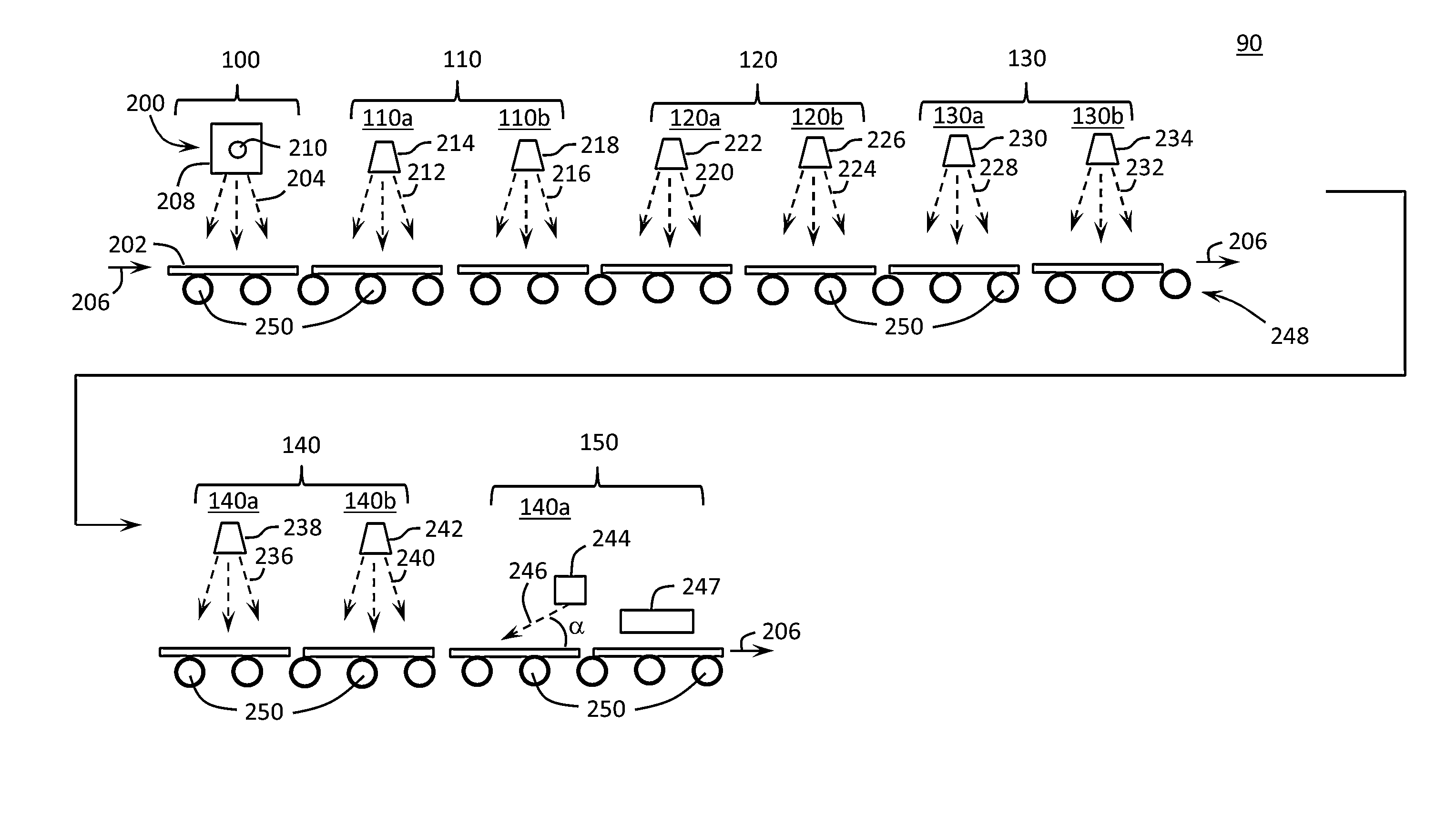
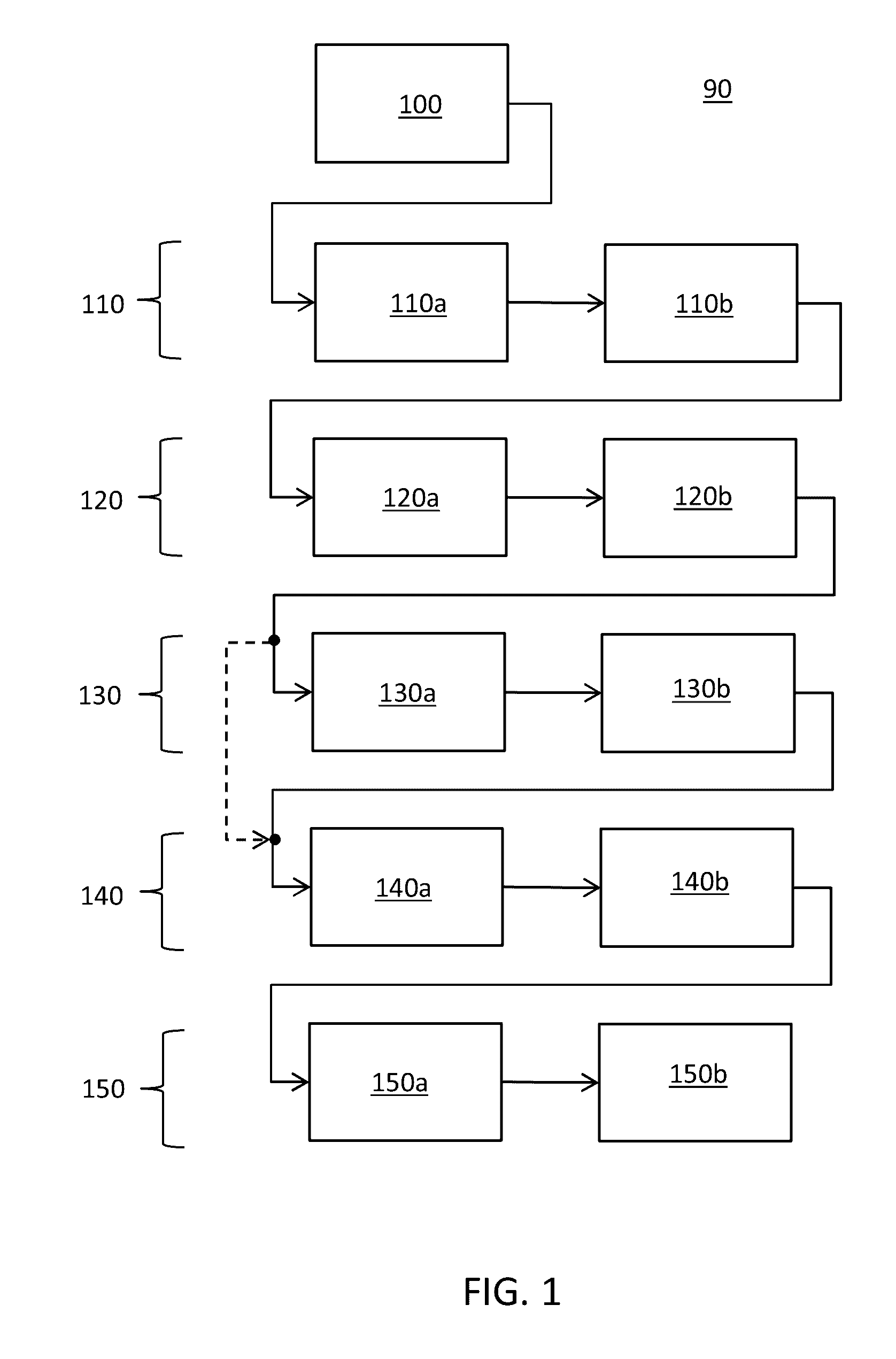
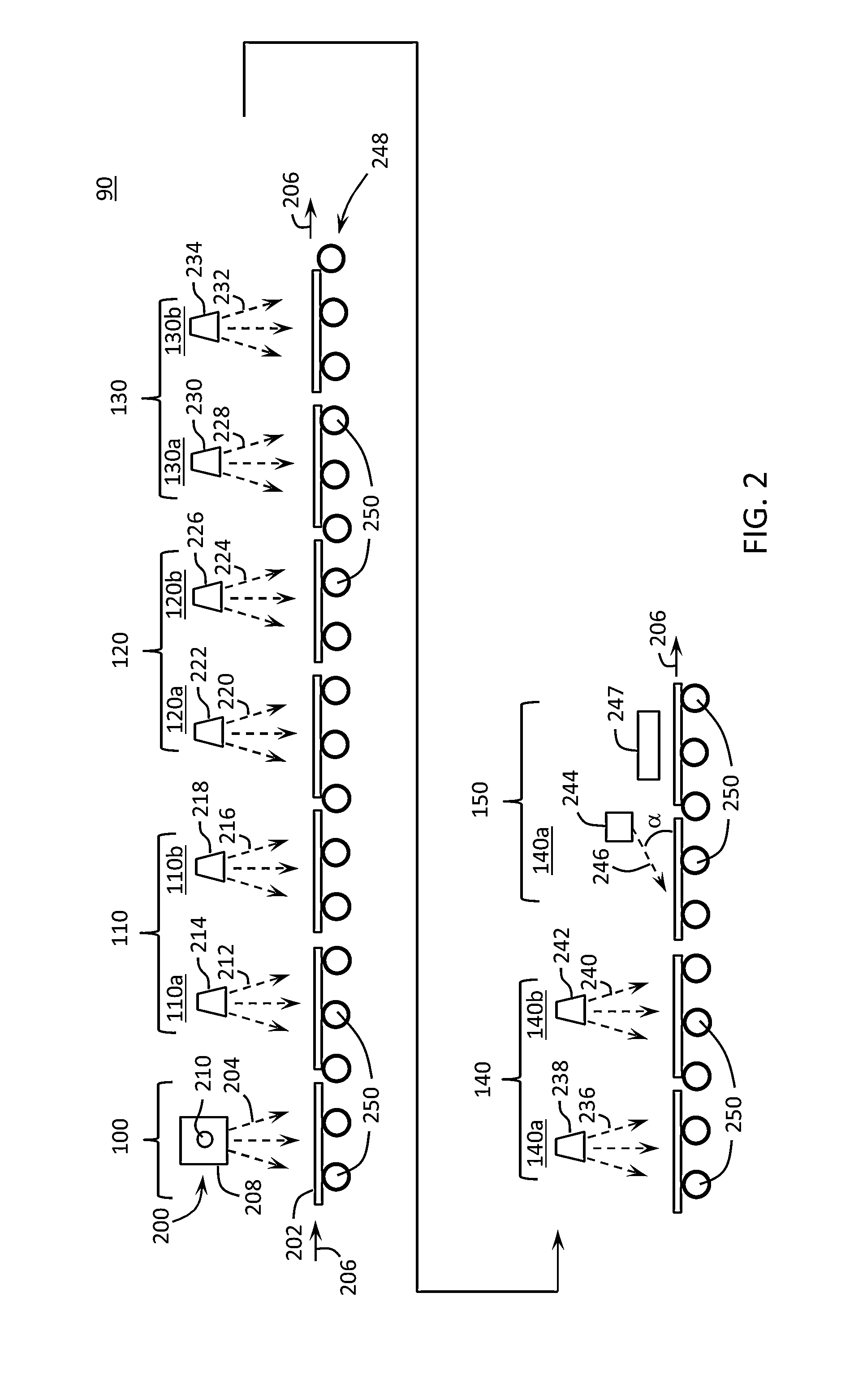
[0036]An exemplary process for manufacturing a glass substrate, and in particular a thin glass substrate suitable for the manufacture of liquid crystal or other type displays, can involve the following steps: (i) forming a thin ribbon of glass, (ii) cutting the thin ribbon of glass into individual glass substrates (iii) removing areas of non-uniform thickness, e.g. “beads”, that may have developed along the edges of the thin glass ribbon during the forming process, (iv) sizing the glass substrate to required dimensions, (v) peeling of any protective film that may have been attached to the glass substrate, such as for ease in handling, (vi) grinding & polishing edge portions of the glass substrate, such as edge ...


PUM

PropertyMeasurementUnit
frequencyaaaaaaaaaa
molar concentrationaaaaaaaaaa
surface roughnessaaaaaaaaaa

Abstract

A method of cleaning thin glass substrates comprises applying a sequence of chemical washing steps as the thin glass substrate is being conveyed in a conveyance direction. In addition, surfaces of the glass substrate may be treated to enhance electrostatic discharge properties of the glass substrates.

Description

PRIORITY[0001]This application claims the benefit of priority under 35 U.S.C. §119 of U.S. Provisional Application Ser. No. 61 / 817,532 filed on Apr. 30, 2013, the content of which is relied upon and incorporated herein by reference in its entirety.BACKGROUND[0002]Field[0003]This invention generally relates to cleaning of glass articles, and in particular glass substrates used in the manufacture of high performance display panels.[0004]Technical Background[0005]As the line widths of thin film transistors on glass substrates become thinner, technology that removes submicron sized particles effectively so that the transistor is not interrupted by the existence of these contaminants are increasingly in demand. The same can be said for the color filter industry, as contaminants are known to adversely affect black matrix adhesion and resulting RGB pixel integrity. For example, for the color filter industry it is known that black matrix peeling events occur more frequently with narrower li...

Claims


Application Information

Patent Timeline
Patent Type & Authority Patents(United States)
IPC IPC(8): C03C23/00H01L21/02B08B3/08B08B3/12B08B11/04
CPCC03C23/0075B08B3/08B08B3/12B08B11/04H01L21/02041
Inventor ENICKS, DARWIN GENENAKAMURA, YOSHIHIROVENKATACHALAM, SIVAWALCZAK, WANDA JANINAWANG, LIMING
Owner CORNING INC
Why Eureka
Try Eureka