
Semiconductor device package and method of making the same

Active Publication Date: 2017-02-07
ADVANCED SEMICON ENG INC
View PDF2 Cites 0 Cited by
  • Summary
  • Abstract
  • Description
  • Claims
  • Application Information

AI Technical Summary

Benefits of technology

The patent text describes a semiconductor device package that includes a substrate and a semiconductor device with two contact pads on the substrate surface. The package also includes conductive bar and pillar structures on the first contact pad and a conductive pillar on the second contact pad. The technical effects of this technical arrangement include increased contact area, improved current spreading, and reduced signal delay in the semiconductor device package. The method of making this package involves mounting the semiconductor device on the substrate, forming a dielectric layer, exposing the second contact pad, and applying a conductive material to fill the hole.

Problems solved by technology

High power semiconductor device present additional challenges in packaging since the resistance of the main current paths (including pads, contacts and traces) of the package should be carefully controlled in order to avoid reduction in efficiency or excessive heating.

Method used


Image

  • Semiconductor device package and method of making the same
  • Semiconductor device package and method of making the same
  • Semiconductor device package and method of making the same

Examples


Embodiment Construction

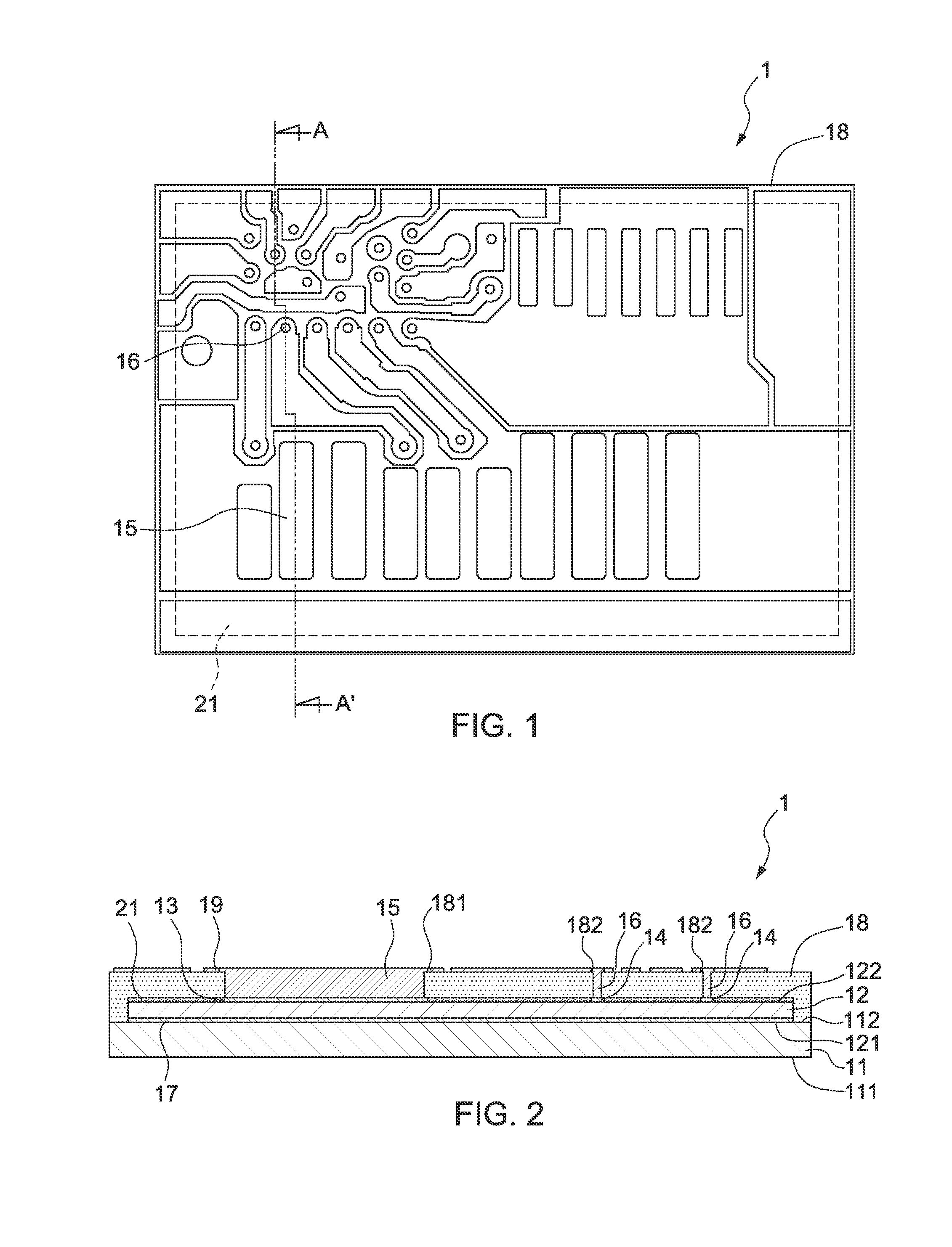
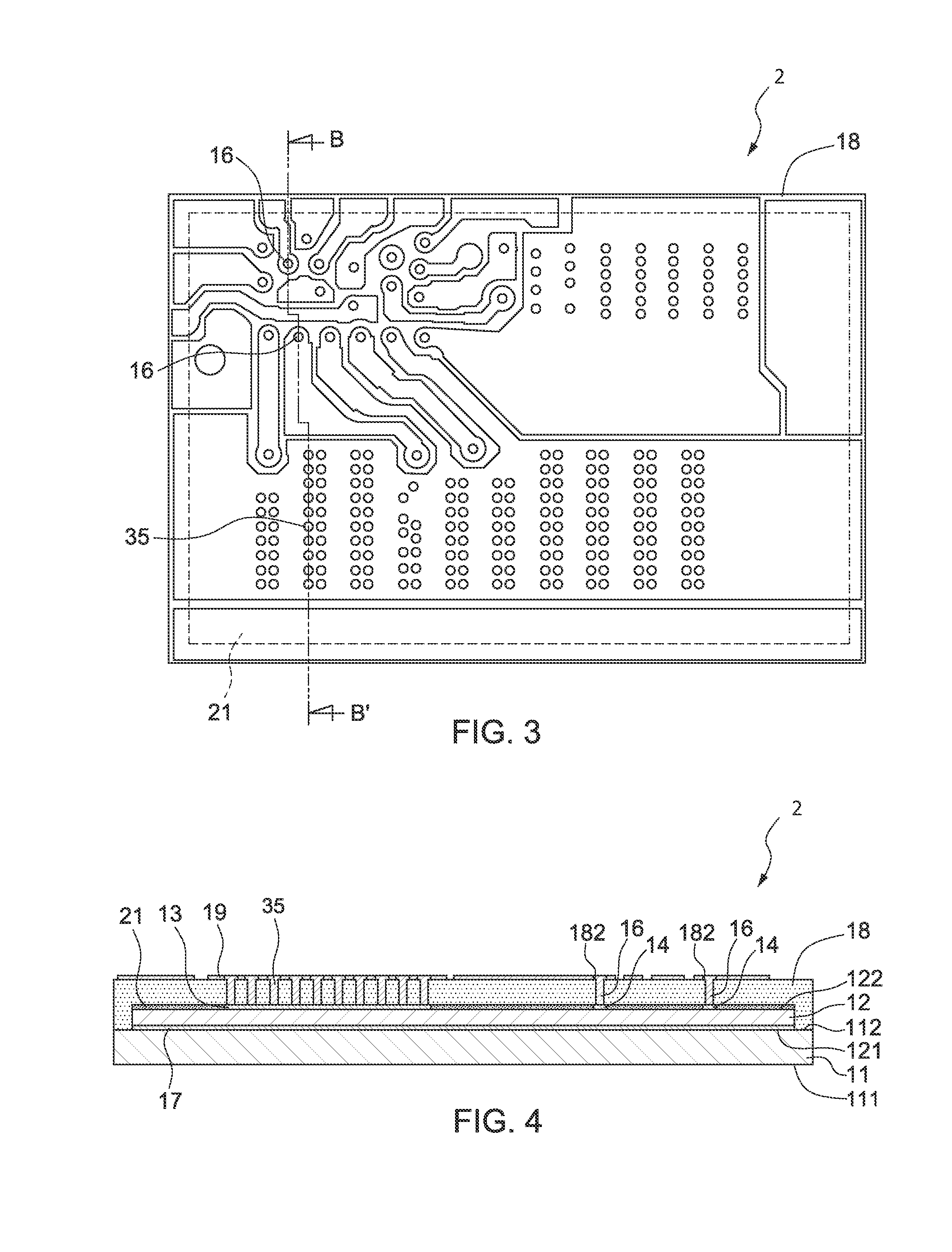
[0018]FIG. 1 illustrates a top view of a semiconductor device package 1 in accordance with an embodiment of the present disclosure. FIG. 2 illustrates a cross-sectional view of the semiconductor device package 1 across line AA′ of FIG. 1. Referring to FIGS. 1 and 2, the semiconductor device package 1 includes a substrate 11, a semiconductor device 12, an insulating layer 21, contact pads 13, 14, 17, conductive bars 15, conductive pillars 16, a dielectric layer 18 and a patterned conductive layer 19.

[0019]The substrate 11 has a surface 111 and a surface 112 opposite the surface 111. The substrate 11 may be a monocrystalline silicon substrate, a polycrystalline silicon substrate, an amorphous silicon substrate, a microcrystalline silicon substrate or a substrate made of another suitable material. The substrate 11 may be a supporting substrate (core substrate) for mounting a number of chips or dies thereon. The substrate 11 may be formed of an insulating material (such as a resin).

[002...


PUM


Abstract

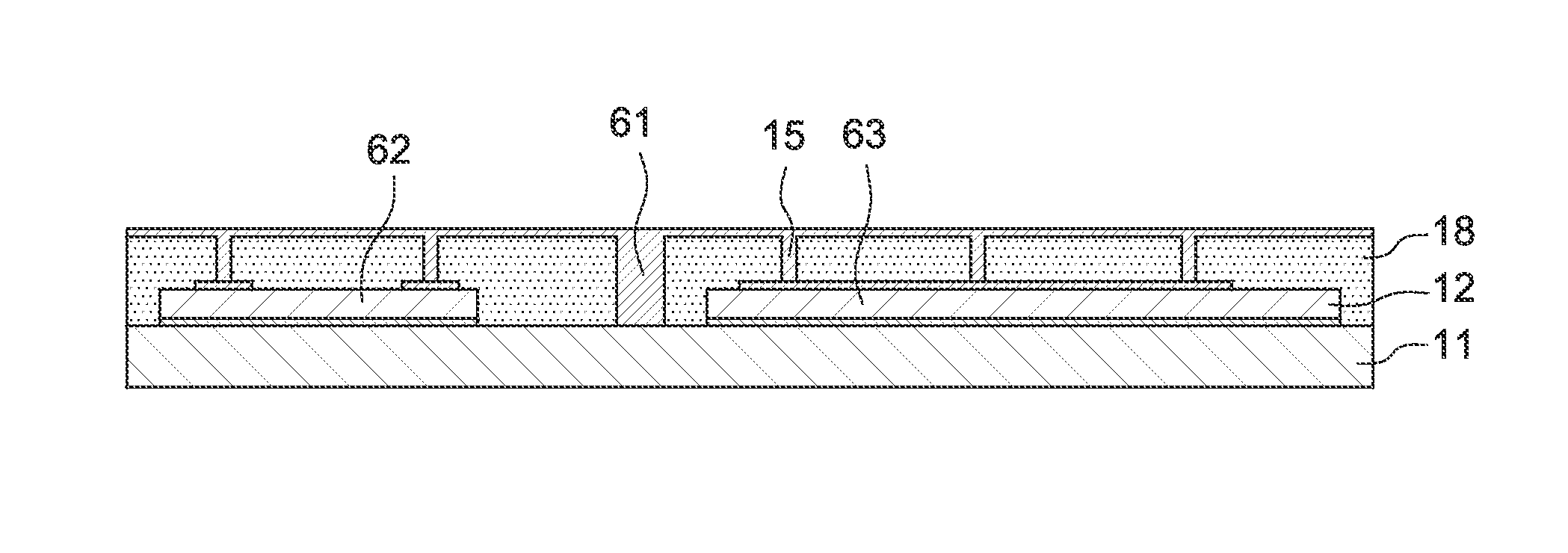
A semiconductor device package includes a substrate and a semiconductor device disposed on a surface of the substrate. The semiconductor device includes a first contact pad and a second contact pad disposed on an upper surface of the semiconductor device. The semiconductor device package further includes a conductive bar disposed on the first contact pad, and a conductive pillar disposed on the second contact pad. A method of making a semiconductor device package includes (a) providing a substrate; (b) mounting a semiconductor device on the substrate, wherein the semiconductor device comprises a first contact pad and a second contact pad on an upper surface of the semiconductor device; (c) forming a dielectric layer on the substrate to cover the semiconductor device; (d) exposing the second contact pad by forming a hole in the dielectric layer; and (e) applying a conductive material over the dielectric layer and filling the hole.

Description

BACKGROUND[0001]1. Technical Field[0002]The present disclosure relates generally to semiconductor device packages and method of making the same. More particularly, the present disclosure relates to high power semiconductor device packages.[0003]2. Description of the Related Art[0004]Semiconductor device packaging has continued to receive a significant amount of attention from designers and manufacturers of electronic products. This attention is based upon the market demand for products with greater efficiency, higher performance, and smaller dimensions.[0005]High power semiconductor device present additional challenges in packaging since the resistance of the main current paths (including pads, contacts and traces) of the package should be carefully controlled in order to avoid reduction in efficiency or excessive heating. High power semiconductor devices may include devices such as field effect transistors (FETs), metal oxide semiconductor FETs (MOSFETs), insulated gate FETs (IGFET...

Claims


Application Information

Patent Timeline
IPC IPC(8): H01L23/00H01L23/498H01L21/52H01L21/768
CPCH01L23/49844H01L21/52H01L21/76802H01L21/76877H01L23/49811H01L23/49827H01L21/486H01L23/5389H01L23/552H01L24/24H01L24/82H01L2224/04105H01L2224/06181H01L2224/24226H01L2224/32225H01L2224/73267H01L2224/92244H01L2924/3025H01L2924/3511H01L2224/8203
Inventor HUANG, CHIH-YICHEN, KUO-HUACHIU, CHI-TSUNG
Owner ADVANCED SEMICON ENG INC
Learn More