

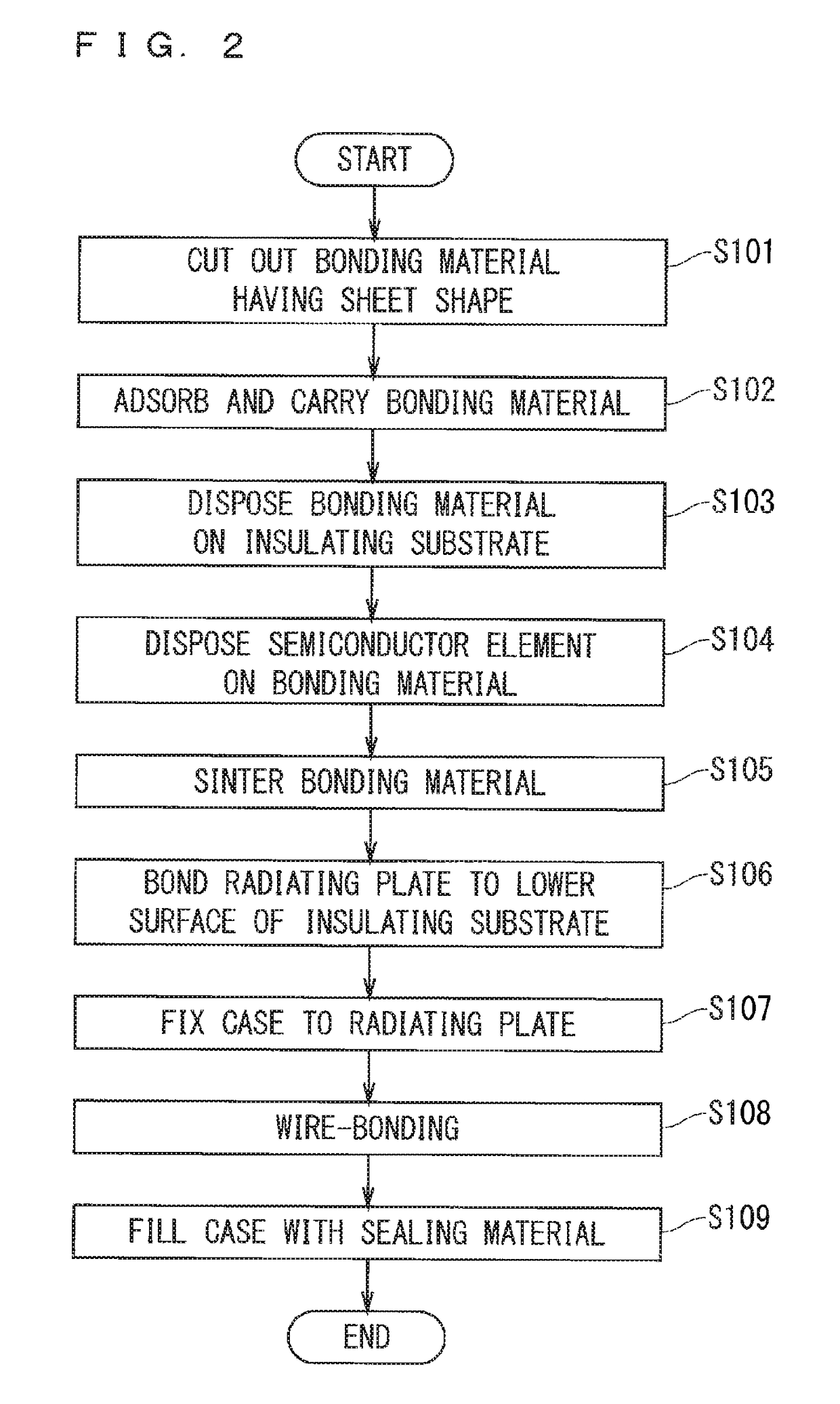
Method for manufacturing semiconductor device
a manufacturing method and semiconductor technology, applied in semiconductor devices, semiconductor/solid-state device details, electrical devices, etc., can solve the problems of difficult to suppress the cost and maintain quality and reliability of bonding, and the thickness of bonding materials is not uniform, so as to achieve high-quality bonding and suppress the cost of bonding materials having sinterability.
- Summary
- Abstract
- Description
- Claims
- Application Information
AI Technical Summary
Benefits of technology
Problems solved by technology
Method used
Image

Examples
first preferred embodiment
[0023]
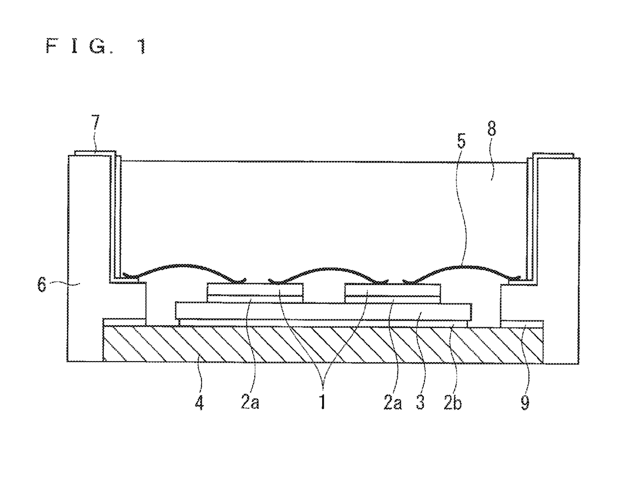
[0024]FIG. 1 is a cross-sectional view of a semiconductor device in a first preferred embodiment. The semiconductor device in this preferred embodiment is a semiconductor element device that is used under high temperature conditions and can operate at high temperature. High temperature herein refers to 175° C. to 200° C. or higher, for example.
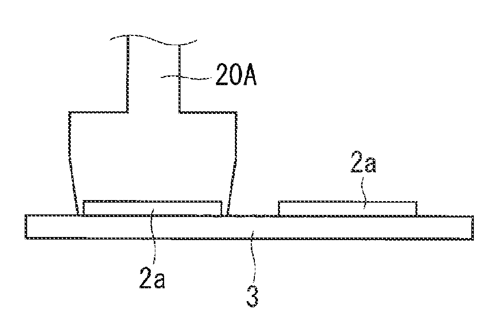
[0025]The semiconductor device in the first preferred embodiment includes an insulating substrate 3 being a substrate having insulation performance, semiconductor elements 1 bonded to the insulating substrate 3, and a bonding material 2a having sinterability that bonds the insulating substrate 3 and the semiconductor elements 1. A circuit pattern is formed on a surface of the insulating substrate 3. The circuit pattern is bonded to back surface electrodes of the semiconductor elements 1 with the bonding material 2a having the sinterability.
[0026]A surface of the insulating substrate 3 opposite to the semiconductor elements 1 is bonded to...
second preferred embodiment
[0066]
[0067]FIG. 7 is a cross-sectional view of a semiconductor device in a second preferred embodiment. The semiconductor device in the second preferred embodiment is a semiconductor element device that is used under high temperature conditions and can operate at high temperature, similarly to the first preferred embodiment.
[0068]The semiconductor device in the second preferred embodiment includes a conductive substrate 10, semiconductor elements 1 bonded to the conductive substrate 10, and a bonding material 2a having sinterability that bonds the conductive substrate 10 and the semiconductor elements 1. In addition, the conductive substrate 10 is a metal plate. The bonding material 2a in the second preferred embodiment is the same bonding material as that in the first preferred embodiment.
[0069]A back surface of the conductive substrate 10 (namely, a surface opposite to a surface bonded to the semiconductor elements 1) adheres to a metal insulating layer 11 including an insulating...
PUM
| Property | Measurement | Unit |
|---|---|---|
| temperature | aaaaa | aaaaa |
| temperature | aaaaa | aaaaa |
| thickness | aaaaa | aaaaa |
Abstract
Description
Claims
Application Information