Electronic device, structure, and heat sink

a technology of electronic devices and heat sinks, applied in the direction of waveguide devices, modification by conduction heat transfer, cross-talk/noise/interference reduction, etc., can solve the problem of limiting the compounding ratio of magnetic materials and dielectric materials, unable to freely control frequency having an electromagnetic wave suppression effect, and unable to suppress radiation noise in arbitrary frequency

Active Publication Date: 2017-04-18
NEC CORP
View PDF16 Cites 2 Cited by
  • Summary
  • Abstract
  • Description
  • Claims
  • Application Information

AI Technical Summary

Benefits of technology

[0015]The present invention relates to an electronic device which includes a substrate and a heat sink, and an object thereof is to provide an electronic device which can suppress radiation noise of arbitrary frequency without generating a decrease of a thermal contact between the heat sink and an electronic circuit.
[0022]According to the present invention, in the electronic device including the substrate and the heat sink, the electronic device is realized in which radiation noise in arbitrary frequency can be suppressed without decreasing thermal contact between the heat sink and the substrate.

Problems solved by technology

However, in the technologies of Patent Documents 1 and 2, the following problems exist.
First, problems of the technology of Patent Document 1 will be described.
A first problem is that in a case of the technology of Patent Document 1 in which the electromagnetic wave absorbing material is inserted between the heat sink and the electronic circuit, the problem in that the electromagnetic wave absorbing material causes the decrease of the thermal contact between the heat sink and the electronic circuit is not essentially solved.
A second problem is that frequency having an electromagnetic wave suppression effect cannot be freely controlled.
However, the compounding ratio of the magnetic materials and the compounding ratio of the dielectric materials are restricted by an object of obtaining sufficient flexibility and electromagnetic wave attenuation effect.

Method used


Image

  • Electronic device, structure, and heat sink
  • Electronic device, structure, and heat sink
  • Electronic device, structure, and heat sink

Examples


first embodiment

[0050]Hereinafter, a first embodiment of the present invention will be described with reference to the drawings.

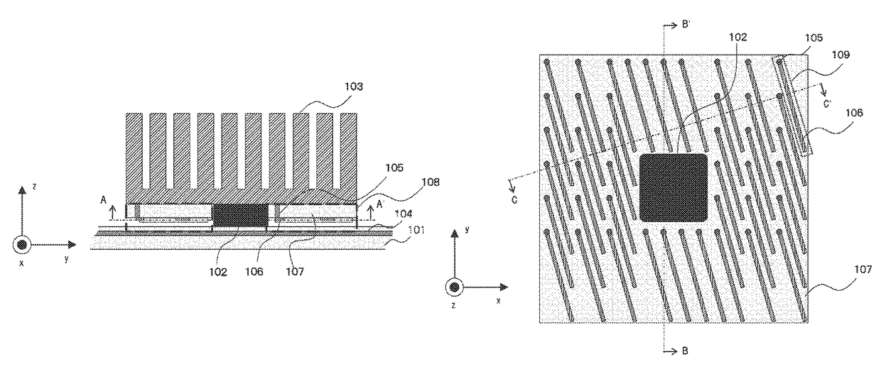
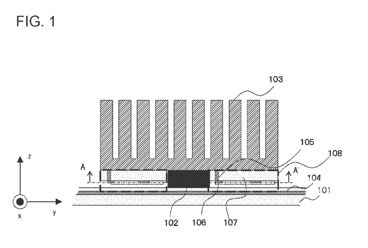
[0051]FIGS. 1 and 2 are cross-sectional views of an electronic device which is the first embodiment of the present invention. FIG. 1 is a cross-sectional view taken along B-B′ of FIG. 2, and FIG. 2 is a cross-sectional view taken along A-A′ of FIG. 1. Moreover, as shown in FIGS. 1 and 2, an x axis, a y axis, and a z axis are defined.

[0052]As shown FIG. 1, the electronic device of the present embodiment includes a substrate 101, an electronic circuit 102, and a heat sink 103. The electronic circuit 102 such as an IC and an LSI is mounted on the substrate 101, and the heat sink 103 is mounted on the electronic circuit 102.

[0053]The substrate 101 includes a conductor plane 104 which is configured of copper, aluminum, or the like on a surface of a side to which the electronic circuit 102 is mounted, or an inner layer. The conductor plane 104 is provided to face the heat sink 1...

second embodiment

[0094]Hereinafter, a second embodiment of the present invention will be described with reference to the drawings. In the present embodiment, the relationship between the stub and the conductor via is different from that of the first embodiment. Other configurations are similar to those of the first embodiment, and here, the descriptions will not be repeated.

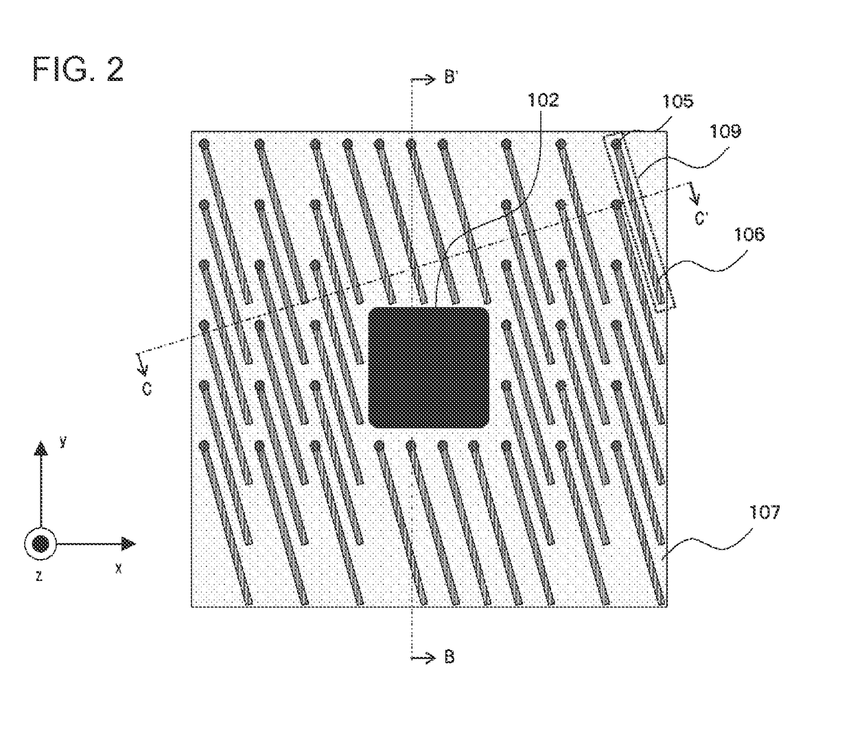
[0095]FIGS. 11 and 12 are plan views showing the relationship between the stub and the conductor via of the present embodiment. In the first embodiment, one stub 106 is connected to one conductor via 105 (refer to FIGS. 2 to 5). On the other hand, in the present embodiment, for example, two stubs 106 and 106′ may be connected to one conductor via 105 (refer to FIG. 11). In addition, in the present embodiment, for example, three stubs 106, 106′, and 106″ may be connected to one conductor via 105 (refer to FIG. 12). Moreover, in the present embodiment, four or more stubs may be connected to one conductor via 105. The planar shape o...

third embodiment

[0104]Hereinafter, a third embodiment of the present embodiment will be described with reference to the drawings. In the present embodiment, the configuration of a space, which is interposed between the substrate 101 including the conductor plane 104 and the dielectric layer 107 in which the conductor via 105 and the stub 106 are formed, is different from those of the first and second embodiments. Other configurations are similar to those of the first or the second embodiment, and here, the descriptions will not be repeated.

[0105]FIG. 15 is a cross-sectional view in which a portion of an electronic device of the present embodiment is extracted. In the first and second embodiments, the cavity filled with air exists in the space which is interposed between the substrate 101 including the conductor plane 104 and the dielectric layer 107 in which the conductor via 105 and the stub 106 are formed (refer to FIG. 1). On the other hand, in the present embodiment, a portion or the whole of t...


PUM


Abstract

An electronic device includes a substrate (101), a conductor plane (104) which is provided on an inner layer of the substrate (101), an electronic circuit (102) which is mounted on the substrate (101), a heat sink (103) which is mounted on an upper surface of the electronic circuit (102), includes a portion which does not overlap with the electronic circuit (102) when seen in a plan view, faces the conductor plane (104), and is configured of a conductive material, a conductor via (105) which is connected to the heat sink (103) on a surface of the heat sink (103) contacting the electronic circuit (102), and extends toward the conductor plane (104), and a stub (106) which is connected to the conductor via (105) and extends to face the conductor plane (104).

Description

CROSS-REFERENCE TO RELATED APPLICATIONS[0001]This application is a national stage application of International Application No. PCT / JP2012 / 002516 entitled “ELECTRONIC DEVICE, STRUCTURE, AND HEAT SINK,” filed on Apr. 11, 2012, which claims the benefit of the priority of Japanese patent application JP2011-130358, filed on Jun. 10, 2011, the disclosures of each of which are hereby incorporated by reference in their entirety.TECHNICAL FIELD[0002]The present invention relates to an electronic device, a structure, and a heat sink.BACKGROUND ART[0003]In an electronic circuit such as an IC or an LSI which is mounted on a substrate, high integration is advanced to realize high speed and high function, and accordingly, a large electric current is consumed. According to heat generation of the large electric current, a heat sink is always provided on the electronic circuit to prevent the electronic circuit from exceeding an allowable temperature. For example, the heat sink is configured of a met...

Claims


Application Information

Patent Timeline
Patent Type & Authority Patents(United States)
IPC IPC(8): H05K7/20H01P1/20H01L23/36H01L23/552H05K1/02H01L23/367H01L23/64
CPCH01L23/36H01L23/3677H01L23/552H05K7/2039H01P1/2005H05K1/0236H01L23/3672H01L23/64H01L2924/0002H05K1/0203H01L2924/00
Inventor KASAHARA, YOSHIAKITOYAO, HIROSHI
Owner NEC CORP
Why Eureka
Try Eureka