Printed circuit board and printed wiring board

a printed circuit board and wiring board technology, applied in the direction of printed circuit non-printed electric components association, sustainable manufacturing/processing, final product manufacturing, etc., can solve the problems of malfunction, power supply terminals not being connected with different dc, and power supply potential fluctuation caused by malfunction, etc., to reduce the number of layers of printed wiring boards, suppress radiation noise, and reduce power supply potential fluctuation

Active Publication Date: 2013-12-26
CANON KK
View PDF9 Cites 3 Cited by
  • Summary
  • Abstract
  • Description
  • Claims
  • Application Information

AI Technical Summary

Benefits of technology

[0010]Therefore, it is an object of the present invention to reduce the number of layers of a printed wiring board while reducing a power supply potential fluctuation and suppressing radiation noise when an LSI requiring multiple power supplies is mounted on the printed wiring board.

Problems solved by technology

In recent years, along with an increase in current consumption of a large-scale integration (hereinafter referred to as “LSI”) as a semiconductor package, a malfunction of the LSI caused by a power supply potential fluctuation has been a problem.
If a power supply potential fluctuation is large, a power supply voltage for driving the LSI becomes short so that a malfunction may occur.
Further, the power supply potential fluctuation propagates to a cable or the like connected to a printed circuit board, and radiation noise is generated from the cable or the like as an antenna so as to cause a malfunction of peripheral electronic devices.
Therefore, it is not possible to connect the power supply terminals of the LSI applied with different DC voltages to the power supply patterns on the surface layer.
Therefore, it is not possible to reduce the number of layers of the printed wiring board.

Method used


Image

  • Printed circuit board and printed wiring board
  • Printed circuit board and printed wiring board
  • Printed circuit board and printed wiring board

Examples


first embodiment

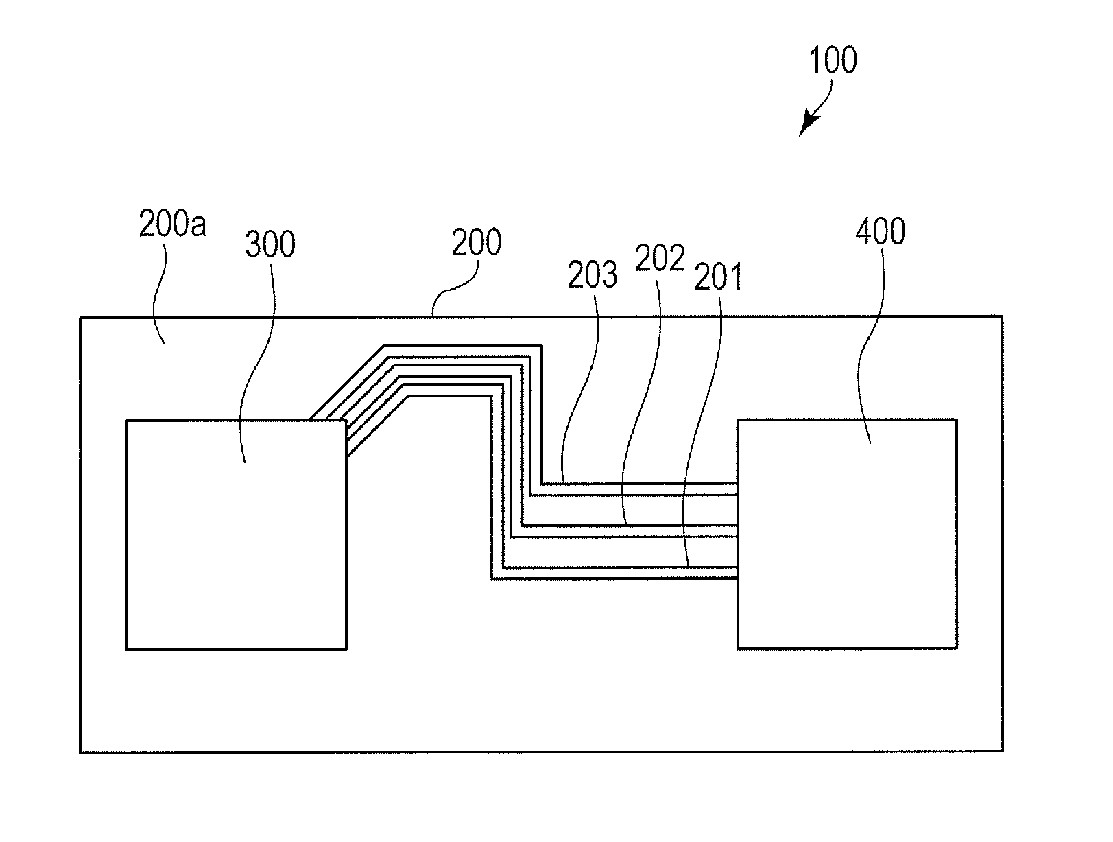
[0030]FIG. 1 is a plan view illustrating a schematic structure of a printed circuit board according to a first embodiment of the present invention. A printed circuit board 100 illustrated in FIG. 1 includes a printed wiring board 200, an LSI 300 as a semiconductor package that is mounted on another layer 200a of the printed wiring board 200, and a power supply circuit 400 that is mounted on the surface layer 200a and supplies power to the LSI 300.

[0031]The LSI 300 is an LSI that requires multiple power supplies, namely an LSI that operates when multiple different DC voltages are applied. The power supply circuit 400 supplies the multiple different DC voltages.

[0032]The LSI 300 and the power supply circuit 400 are electrically connected by first to third main power supply patterns 201 to 203 as conductor patterns disposed on the surface layer 200a of the printed wiring board 200. The power supply circuit 400 applies the multiple different DC voltages to the LSI 300 via the main power...

second embodiment

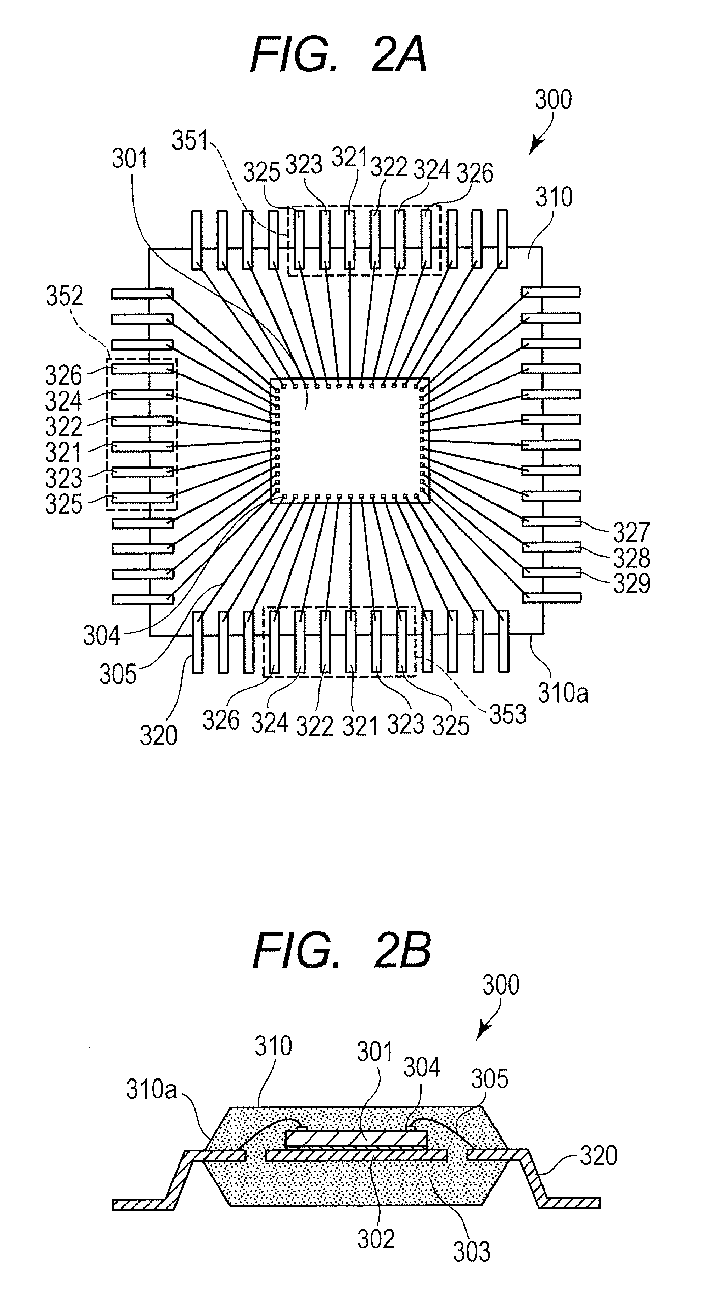
[0062]Next, a printed circuit board according to a second embodiment of the present invention is described. FIG. 5 is a plan view of the printed wiring board in a vicinity of the LSI according to the second embodiment of the present invention. In the second embodiment, the same structure as that of the first embodiment is denoted by the same numeral or symbol so that overlapping description is omitted.

[0063]In the first embodiment, there is described the case where the first power supply pattern 211 is formed in a single stroke manner as illustrated in FIG. 3. However, the present invention is not limited thereto, and as illustrated in FIG. 5, a power supply pattern 211A may not be formed in a single stroke manner.

[0064]In the second embodiment, an LSI 300A includes two terminal groups 351A and 352A as the multiple terminal groups. The terminal group 351A includes one power supply terminal 321A applied with a DC voltage different from those applied to the other power supply terminal...

third embodiment

[0067]Next, a printed circuit board according to a third embodiment of the present invention is described. FIG. 6 is a plan view of the printed wiring board in a vicinity of the LSI according to the third embodiment of the present invention. In the third embodiment, the same structure as that of the first and second embodiments is denoted by the same numeral or symbol so that overlapping description is omitted.

[0068]In the first embodiment, there is described the case where the power supply patterns 211 to 213 are wired via one corner part C1 of the first region R1 as illustrated in FIG. 3. However, the power supply patterns 211 to 213 may be wired via any one of the multiple corner parts.

[0069]In the third embodiment, as illustrated in FIG. 6, the printed wiring board includes first to third main power supply patterns 201B, 202, and 203 which are arranged in the second region R2 on the surface layer 200a and are applied with different DC voltages from the power supply circuit. The ...


PUM


Abstract

On a surface layer of a printed wiring board, main power supply patterns to be applied with different DC voltages are disposed in a second region. Power supply patterns are disposed on the surface layer, and the power supply patterns are led from the main power supply patterns to a first region. The power supply patterns connect power supply terminals of terminal groups in the second region. The power supply patterns connect the power supply terminals between the terminal groups in the first region. Power supply terminals of the terminal groups of a semiconductor package are electrically connected to the main power supply patterns by the power supply patterns. Thus, potential fluctuations are reduced and radiation noise is suppressed, and the number of layers of the printed wiring board is reduced.

Description

BACKGROUND OF THE INVENTION[0001]1. Field of the Invention[0002]The present invention relates to a printed circuit board having a semiconductor package mounted on a printed wiring board, and a printed wiring board having a semiconductor package mounted thereon.[0003]2. Description of the Related Art[0004]In recent years, along with an increase in current consumption of a large-scale integration (hereinafter referred to as “LSI”) as a semiconductor package, a malfunction of the LSI caused by a power supply potential fluctuation has been a problem.[0005]When the LSI operates, a potential fluctuation occurs, which is determined by the product of impedance of a power supply path between the LSI and a power supply circuit, and a current flowing on the power supply path. If a power supply potential fluctuation is large, a power supply voltage for driving the LSI becomes short so that a malfunction may occur. Further, the power supply potential fluctuation propagates to a cable or the like...

Claims


Application Information

Patent Timeline
Patent Type & Authority Applications(United States)
IPC IPC(8): H05K1/18
CPCH05K1/181H05K1/0228H05K1/0262H05K2201/09309H05K2201/10689H01L2224/32245H01L2224/48247H01L2224/73265Y02P70/50H01L2924/00012
Inventor HOSHI, SOUYAMASHITA, NOBUAKIMURAI, YUSUKEOHSAKA, TOHRU
Owner CANON KK
Why Eureka
Try Eureka