

Electrostatic discharge protection device with parasitic bipolar junction transistors
a protection device and bipolar junction technology, applied in semiconductor devices, semiconductor/solid-state device details, electrical apparatus, etc., can solve problems such as non-uniform turn-on problems, circuit errors, and multi-finger ggnmos that cannot be uniformly turned on under esd stress, and achieve esd tolerance and esd robustness of esd protection devices. the effect of further enhancemen
- Summary
- Abstract
- Description
- Claims
- Application Information
AI Technical Summary
Benefits of technology
Problems solved by technology
Method used
Image

Examples
Embodiment Construction
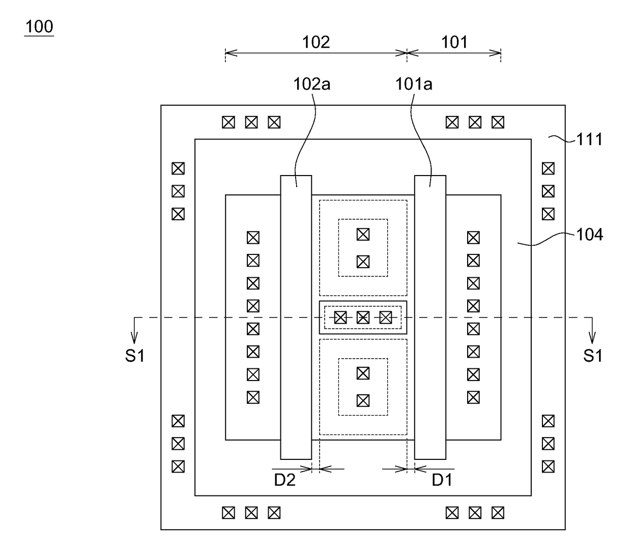
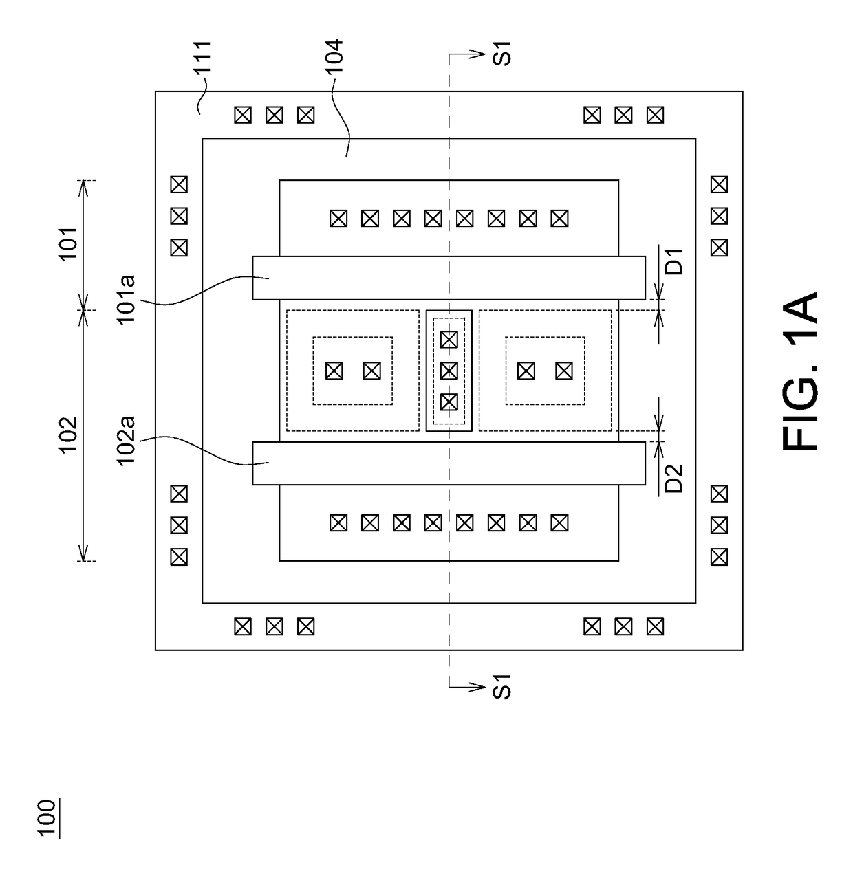
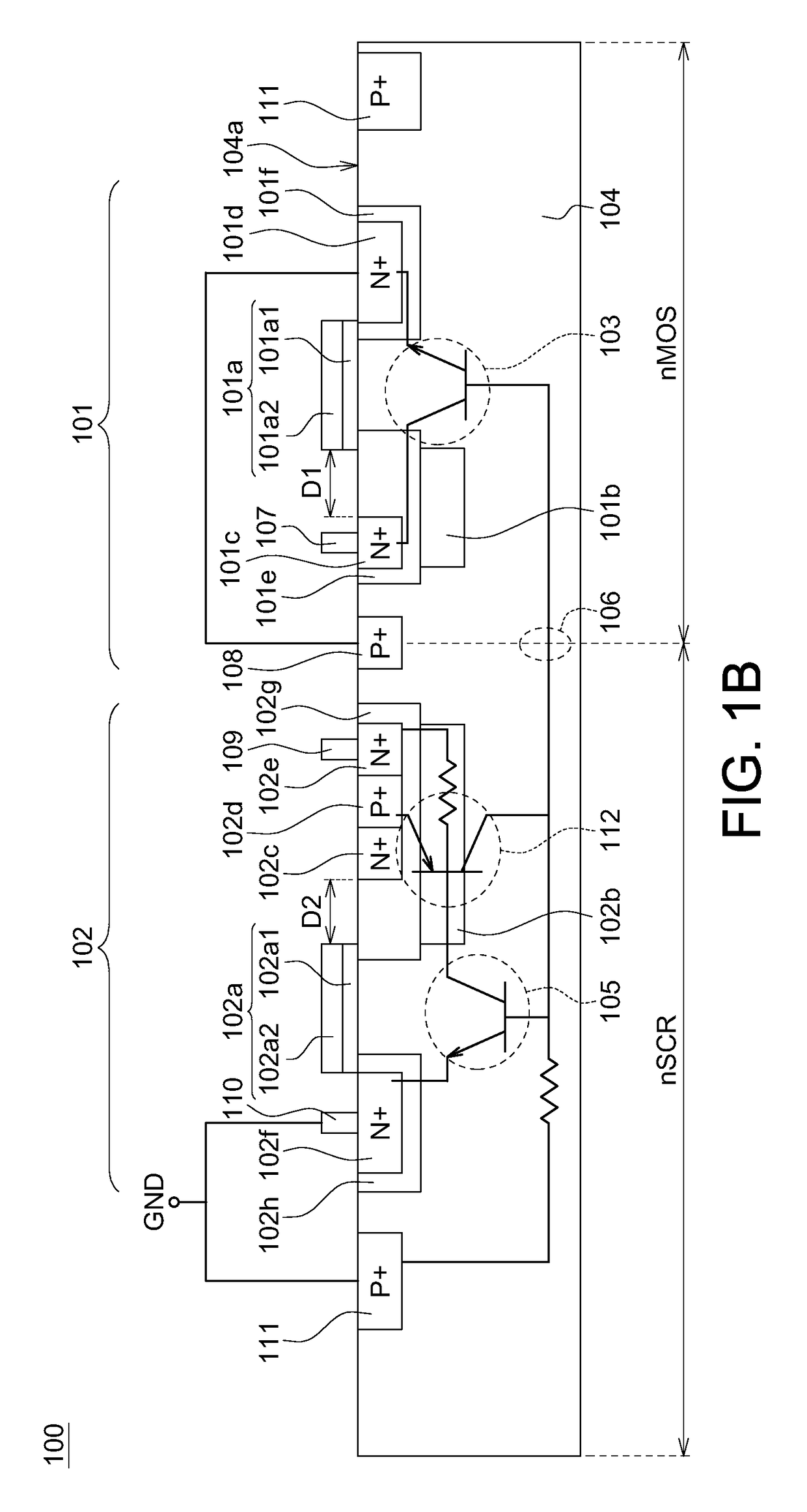
[0021]The embodiments as illustrated below provide an ESD protection device to solve the problems of turn-on uniformity and ESD robustness under ESD stress. The present invention will now be described more specifically with reference to the following embodiments illustrating the structure and arrangements thereof.
[0022]It is to be noted that the following descriptions of preferred embodiments of this invention are presented herein for purpose of illustration and description only. It is not intended to be exhaustive or to be limited to the precise form disclosed. Also, it is also important to point out that there may be other features, elements, steps and parameters for implementing the embodiments of the present disclosure which are not specifically illustrated. Thus, the specification and the drawings are to be regard as an illustrative sense rather than a restrictive sense. Various modifications and similar arrangements may be provided by the persons skilled in the art within the ...
PUM
 Abstract
Description
Claims
Application Information