
Methods of forming highly p-type doped germanium tin films and structures and devices including the films

a technology of germanium tin and p-type dopant, which is applied in the direction of polycrystalline material growth, crystal growth process, chemically reactive gas growth, etc., to achieve the effect of high tin content and high p-type dopant conten

Active Publication Date: 2017-05-09
ASM IP HLDG BV
View PDF1436 Cites 333 Cited by
  • Summary
  • Abstract
  • Description
  • Claims
  • Application Information

AI Technical Summary

Benefits of technology

The present patent relates to methods of forming p-type doped GeSn films that can be used in various electronic and photonic devices. The methods involve adding n-type dopant and p-type dopant precursors to a reaction chamber and using a gas-phase reactor to grow the film. The resulting films have a high level of tin and p-type dopant content, and can be used for low ohmic contact resistance. The methods can provide increased levels of one or both dopants in the film, and can be used to form epitaxial layers of p-type doped GeSn overlying a substrate. The films can also include additional layers such as silicon or carbon. The technical effects of the patent include improved methods for forming p-type doped GeSn films with high levels of dopants, and the resulting films can be used for various electronic and photonic applications.

Problems solved by technology

Unfortunately, during p-type doped GeSn film formation, the p-type dopant and the Sn can compete with each other for inclusion in the film.

Method used


Image

  • Methods of forming highly p-type doped germanium tin films and structures and devices including the films
  • Methods of forming highly p-type doped germanium tin films and structures and devices including the films
  • Methods of forming highly p-type doped germanium tin films and structures and devices including the films

Examples


Embodiment Construction

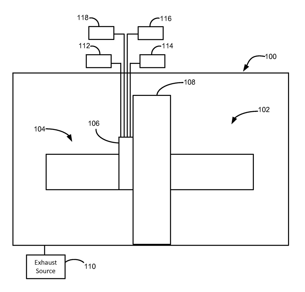
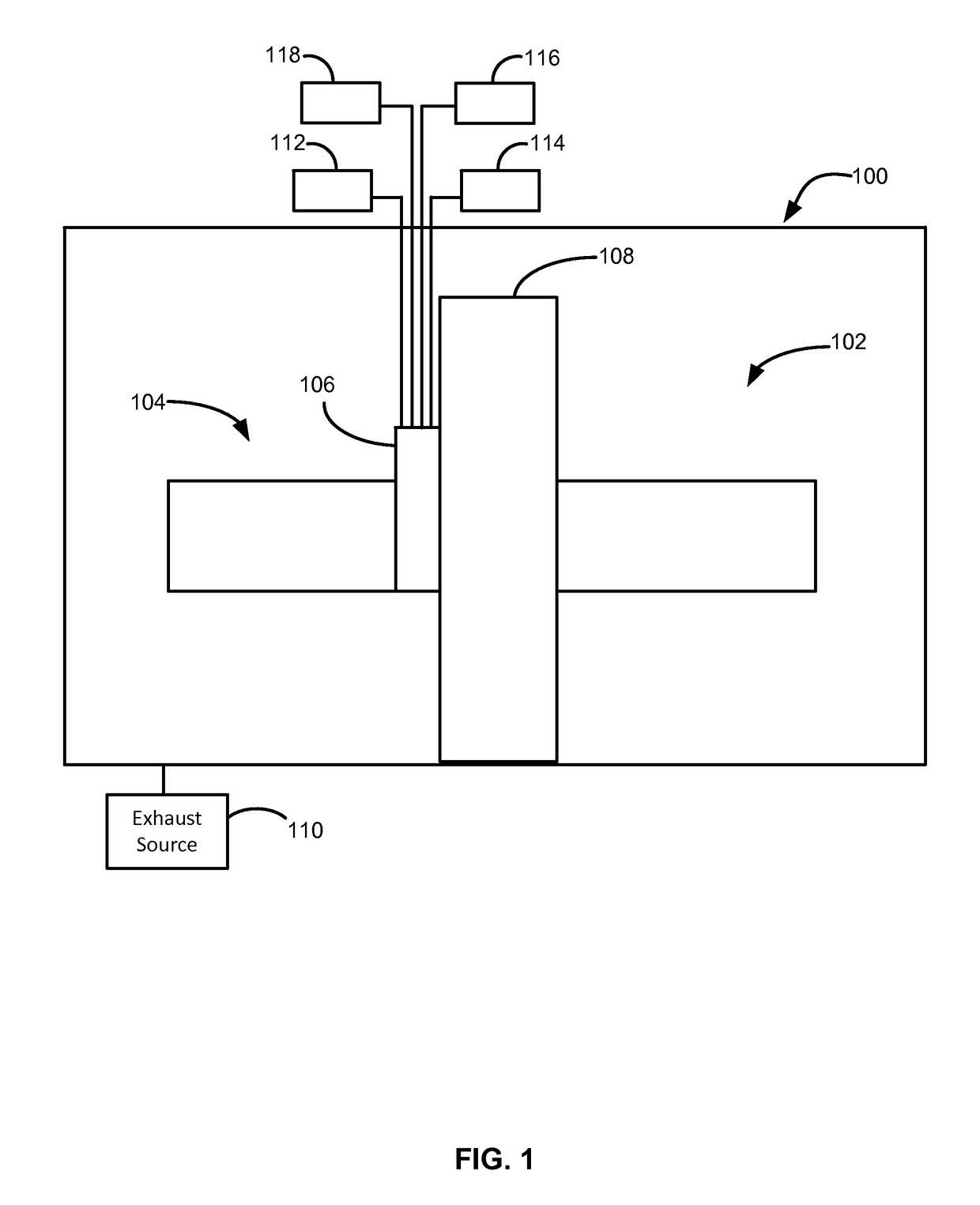
[0026]The description of exemplary embodiments of methods, systems, structures, and devices provided below is merely exemplary and is intended for purposes of illustration only; the following description is not intended to limit the scope of the disclosure or the claims. Moreover, recitation of multiple embodiments having stated features is not intended to exclude other embodiments having additional features or other embodiments incorporating different combinations of the stated features.

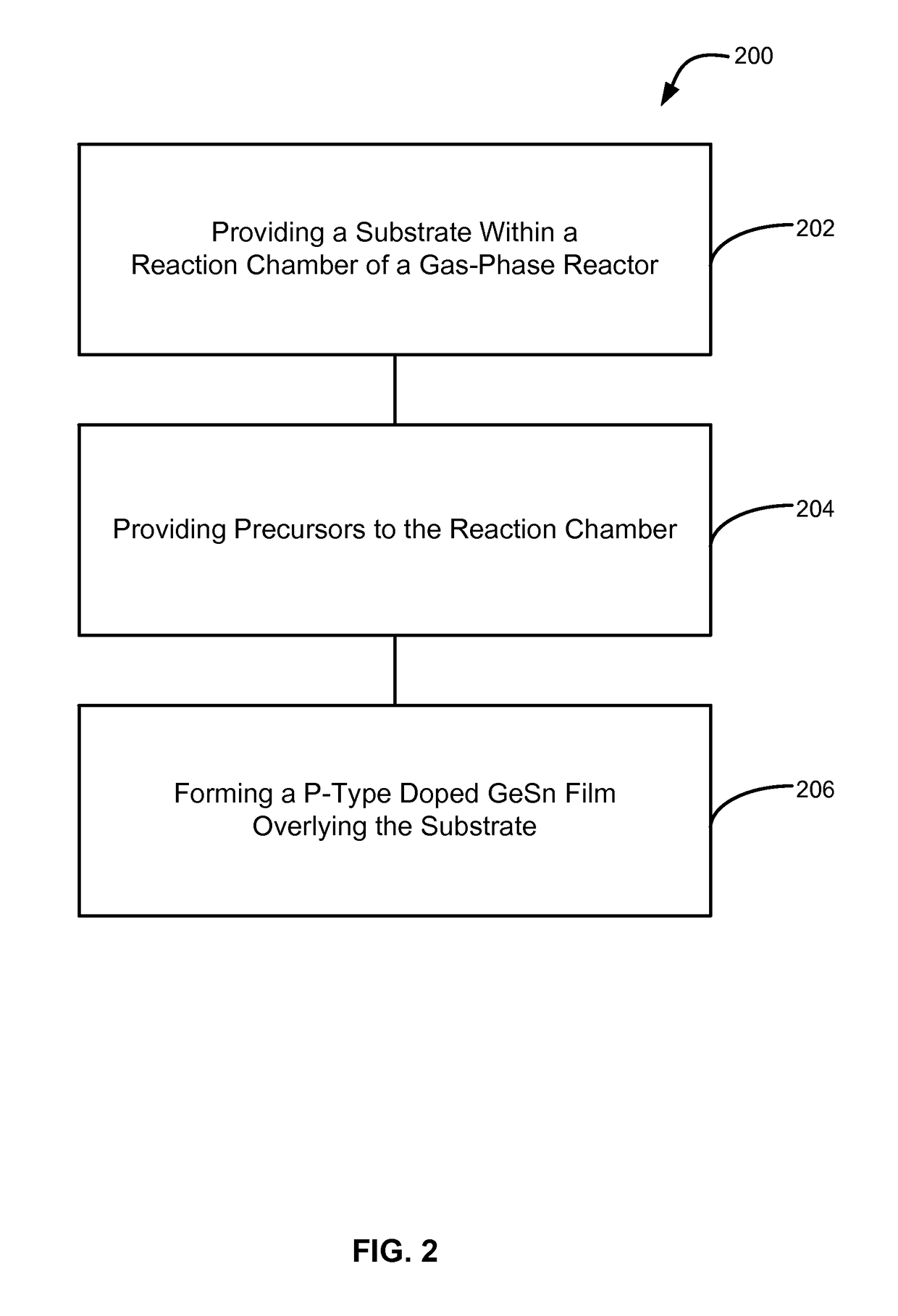
[0027]Exemplary methods in accordance with the present disclosure relate to methods of forming p-type doped GeSn (e.g., crystalline) layers overlying a substrate. The p-type doped GeSn layers may include additional elements, such as silicon and / or carbon, which form part of a crystalline lattice with the p-type doped GeSn layer. As set forth in more detail below, the p-type doped GeSn layer also includes an n-type dopant. Inclusion of the n-type dopant allows increased concentrations of Sn and / or th...


PUM

PropertyMeasurementUnit
pressuresaaaaaaaaaa
pressuresaaaaaaaaaa
pressuresaaaaaaaaaa

Abstract

Methods of forming p-type doped germanium-tin layers, systems for forming the p-type doped germanium-tin layers, and structures including the p-type doped germanium-tin layers are disclosed. The p-type doped germanium-tin layers include an n-type dopant, which allows relatively high levels of tin and / or p-type dopant to be included into the p-type doped germanium-tin layers.

Description

FIELD OF INVENTION[0001]The present disclosure generally relates to techniques for forming layers including germanium tin and to structures and devices including such layers. More particularly, the disclosure relates to methods of forming p-type doped germanium-tin layers, to methods of forming structures and devices including the layers, to systems for forming the layers and structures, and to structures and devices including the layers.BACKGROUND OF THE DISCLOSURE[0002]Various electronic devices, such as semiconductor devices, and photonic devices, such as lasers and solar devices, may include or may desirably include germanium-tin (GeSn) layers, such as GeSn, GeSnSi, GeSnSiC, and the like. For example, GeSn layers can be used to form direct bandgap devices and / or may be used as a stressor to provide strain in an adjacent germanium layer to increase mobility in the germanium layer. Similarly, GeSnSi and / or GeSnSiC layers can be used to form tunable band gap devices as well as opti...

Claims


Application Information

Patent Timeline
Patent Type & Authority Patents(United States)
IPC IPC(8): C23C16/00H01L29/78H01L29/161H01L21/02H01L29/167H01L29/08C23C16/455
CPCH01L29/7848C23C16/455H01L21/0262H01L21/02524H01L21/02579H01L29/0847H01L29/161H01L29/167C23C16/0272C23C16/30C23C16/45512C30B25/02C30B29/52H01L21/02535H01L21/02532H01L21/02576H01L21/02109H01L21/02208H01L21/02129H01L29/785
Inventor MARGETIS, JOETOLLE, JOHN
Owner ASM IP HLDG BV
Learn More