Multilayer inductor

a multi-layer inductor and inductor technology, applied in the direction of fixed inductances, transformer/inductance details, etc., can solve the problems of increasing the whole of the multi-layer inductor, increasing the cost of metal materials, and affecting etc., to achieve the effect of improving the conversion efficiency of converters, improving dc superposition characteristics, and easy saturation

Active Publication Date: 2017-05-16
NJ COMPONENTS CO LTD
View PDF6 Cites 0 Cited by
  • Summary
  • Abstract
  • Description
  • Claims
  • Application Information

AI Technical Summary

Benefits of technology

[0018]In the invention recited in any of claims 1 to 5, the permanent magnet layer is disposed over the whole surface of the outside of the coil or the whole surface of the inside of the coil in axial view, and therefore a leakage magnetic flux Z which does not works as a bias magnetic flux Y and has an opposite direction, like a permanent magnet illustrated in FIG. 15, is not generated. As a result, the permanent magnet layer can significantly improve DC superposition characteristics. Additionally, a low-loss material relatively easily saturated can be used as the magnetic body (magnetic layer), and it is possible to achieve the improvement of converter conversion efficiency.
[0019]Furthermore, like the invention recited in claim 4, manufacture can be facilitated by using the material which is capable of being collectively baked at a temperature of 940° C. or less as the magnetic layer, the permanent magnet layer and the nonmagnetic pattern, sintering a laminated body at a low temperature of 940° C. or less to be integrated, and thereafter magnetizing the permanent magnet layer.
[0020]More specifically, like the invention recited in claim 5, it is suitable that the Ni—Zn ferrite based material is used as the magnetic layer, the Zn ferrite based material is used as the nonmagnetic pattern, the low-temperature sintered magnet material obtained by adding Bi2O3 and SiO2 to the Ba ferrite powder or the Sr ferrite powder is used as the permanent magnet layer.

Problems solved by technology

However, the above ferrite generally tends to be low in magnetic flux saturation density, and to be bad in DC superposition characteristics, and therefore it is becoming difficult to follow the electric current increase in the recent mobile market.
However, when the above coil size is increased, increase in the whole of the multilayer inductor is caused, which is against the market request.
However, the chip inductor has disadvantage that the metal material generally has a large loss at a high frequency compared to the ferrite, and that conversion efficiency is reduced in a conversion usage.
Therefore, there is a problem that the bias magnetic flux Y from the permanent magnet 22 does not effectively work, and the DC superposition characteristics can hardly be improved as expected.

Method used


Image

  • Multilayer inductor
  • Multilayer inductor
  • Multilayer inductor

Examples


first embodiment

[0036]FIG. 1 to FIG. 3 each illustrate a first embodiment of a multilayer inductor according to the present invention, and FIG. 4 to FIG. 6 illustrate first to third modifications, respectively.

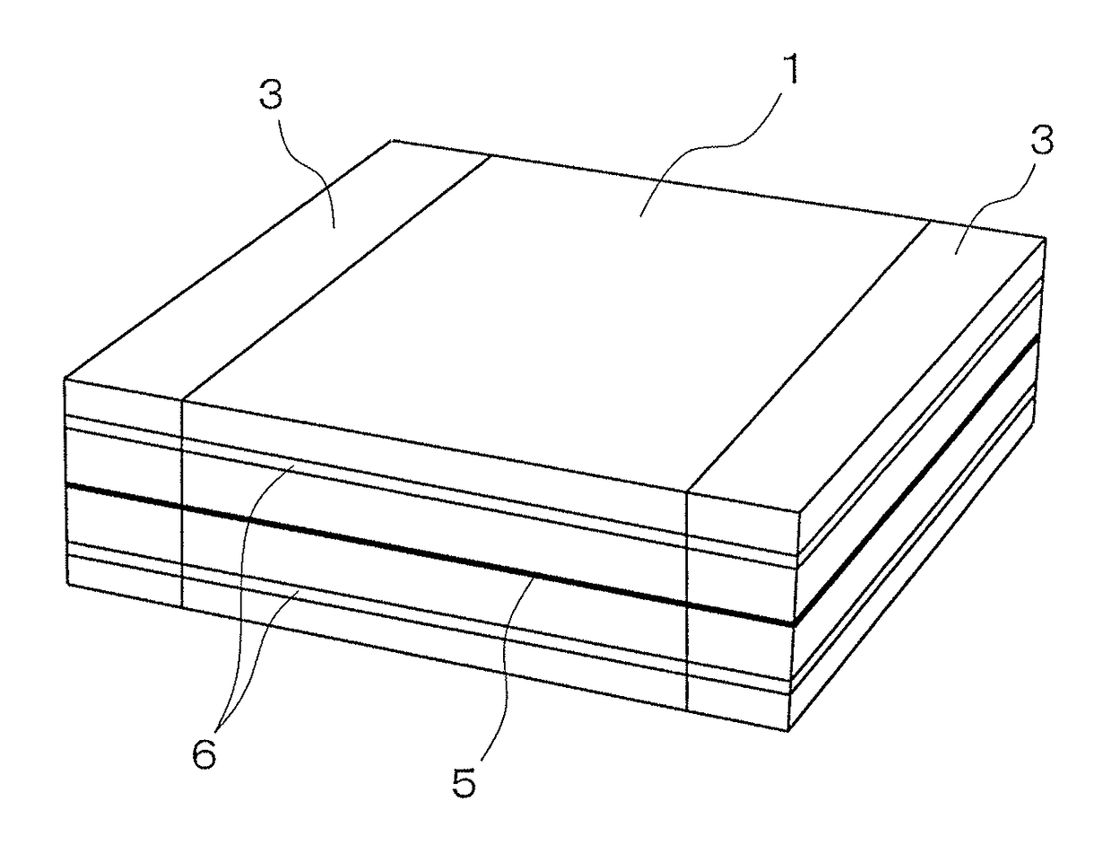
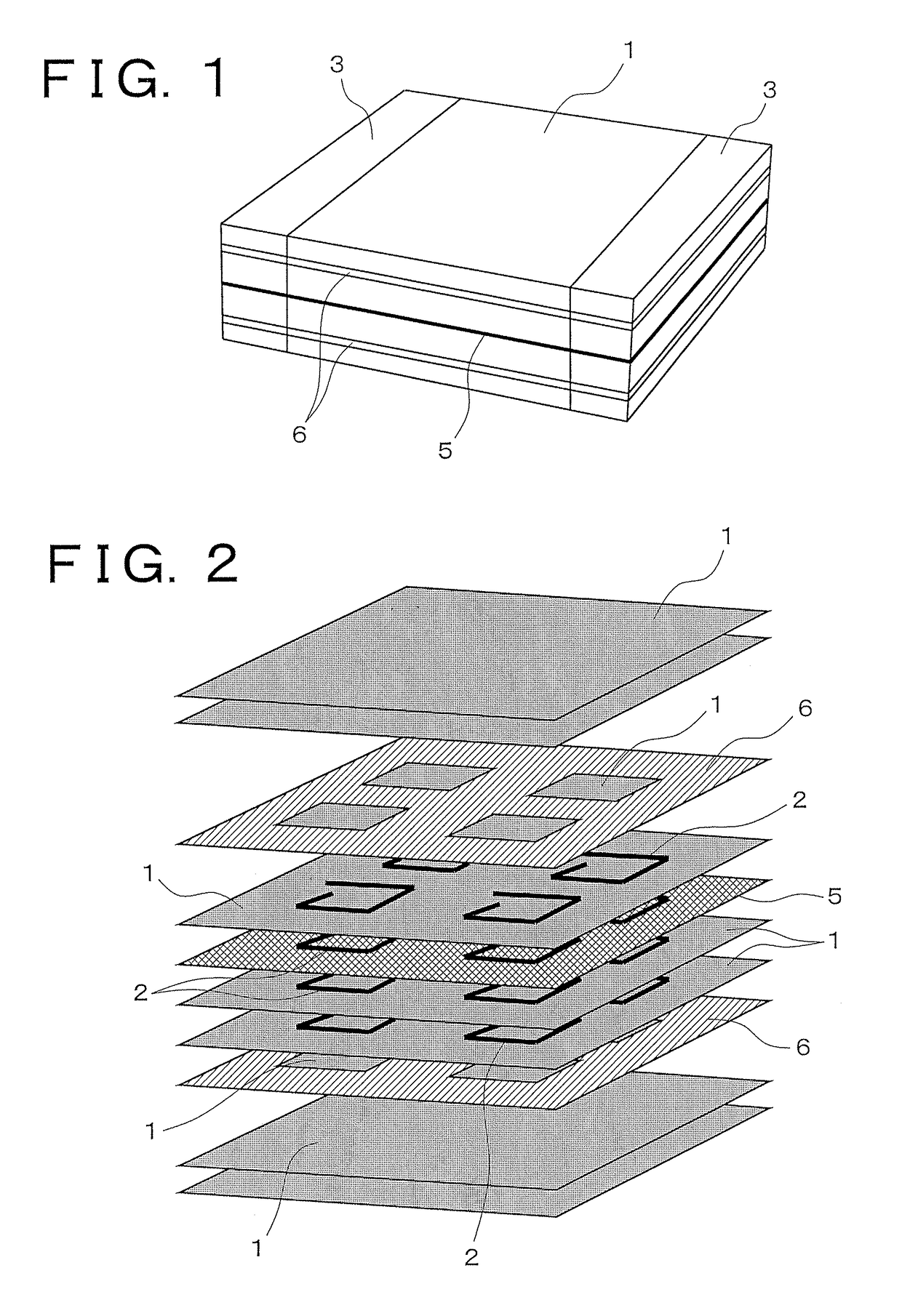
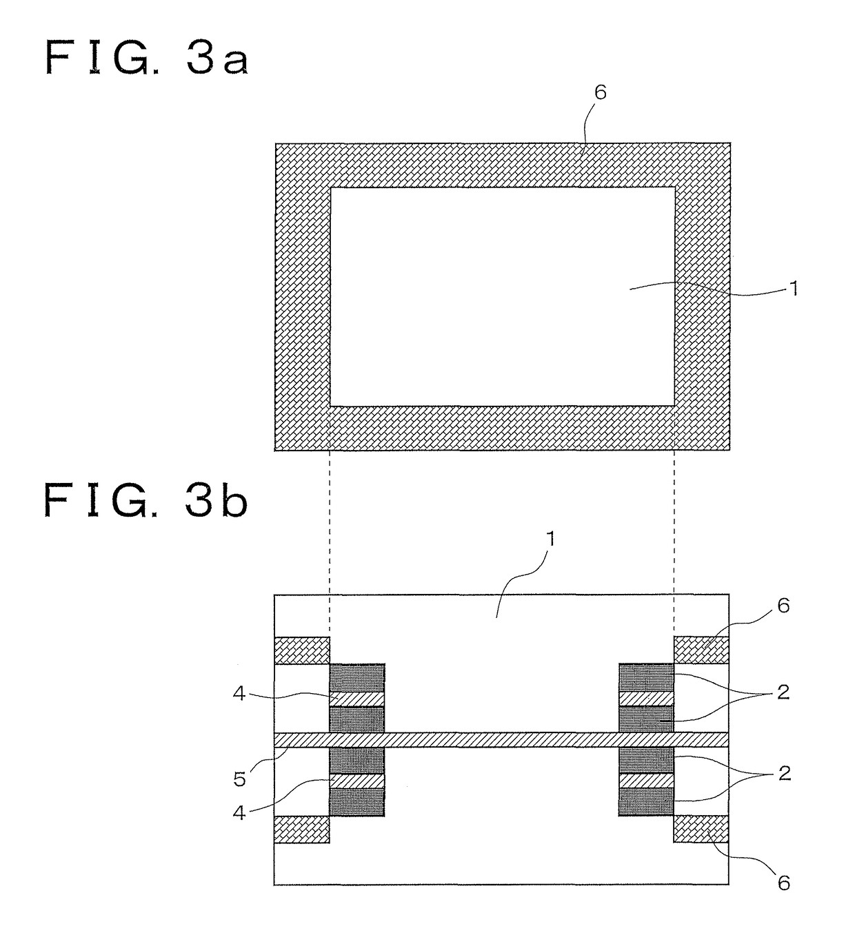
[0037]As illustrated in FIG. 1 to FIG. 3, this multilayer inductor is formed in a rectangular parallelepiped shape, in which a plurality of electrically insulating magnetic layers 1 and conductive patterns 2 are laminated, and each of the conductive patterns 2 is connected in sequence in a lamination direction, so that a spirally circulating coil 2 is formed inside a magnetic body configured by the magnetic layers 1, and both ends of the coil 2 are drawn out to be connected to external electrodes 3. The external electrodes 3 are connected to a land part of a circuit board (not shown), so that the multilayer inductor is surface-mounted.

[0038]Herein, between the conductive patterns 2 adjacent in the lamination direction, an electrically insulating nonmagnetic pattern 4 having a shape correspond...

second embodiment

[0051]FIG. 7 illustrates a second embodiment of a multilayer inductor according to the present invention, and FIG. 8 to FIG. 10 illustrate first to third modifications of the second embodiment, respectively. Hereinafter, the same components as the components illustrated in FIG. 1 to FIG. 6 are denoted by the same reference numerals, and the description thereof is simplified.

[0052]In each of these multilayer inductors, in axial view of a coil 2, a permanent magnet layer 6 magnetized so as to emit a magnetic flux whose direction is opposite to the direction of a magnetic flux excited by the coil 2 is disposed over the whole surface of the inside of the coil 2.

[0053]That is, in the multilayer inductor of the second embodiment, as illustrated in FIG. 7, an annular nonmagnetic pattern 7 made of a Zn ferrite material similar to the nonmagnetic pattern 4 formed between the conductive patterns 2 is formed at a layer above a conductive pattern 2 located at an uppermost layer in the figure in...

example

[0059]In order to verify the effects of the multilayer inductors according to the present invention, the DC superposition characteristics of the multilayer inductors of the present invention, and the DC superposition characteristics of multilayer inductors of comparative examples were obtained to be compared by simulation.

[0060]In both the multilayer inductors of the present invention and the multilayer inductors of the comparative examples, chip size was 2.5×2.0×1.0 mm, the number of turns of the internal conductor was 5 turns, a film thickness of the internal conductor was 120 μm, and the thickness of an insulating layer between the internal conductors was 15 μm.

[0061]First, FIG. 11 illustrates a case where the DC superposition characteristics of multilayer inductors (1) and (2) having the configurations shown in the first embodiment and the first modification are compared with the DC superposition characteristics of a multilayer inductor (3) of a comparative example formed with a...


PUM

PropertyMeasurementUnit
temperatureaaaaaaaaaa
thicknessaaaaaaaaaa

Abstract

A multilayer inductor providing improved DC superposition characteristics by a permanent magnet that emits a bias magnetic flux, and having a low-loss material as a magnetic body to improve converter conversion efficiency. The multilayer inductor has a plurality of laminated electrically insulating magnetic layers; and laminated conductive patterns, each of the conductive patterns being connected in sequence in the lamination direction forming a spiral coil inside the magnetic layer. An magnetized annular permanent magnet layer emits a magnetic flux whose direction is opposite that of a magnetic flux excited by the coil is between an outer peripheral edge of the inductor and an outer peripheral edge of the coil so as not to overlap an inner peripheral part of the magnet layer with the conductive patterns and so as to block a space between the conductive patterns and the magnet layer, in axial view of the coil.

Description

TECHNICAL FIELD[0001]The present invention relates to a suitable multilayer inductor used as an inductor for a DC-DC converter particularly requiring a high bias, or the like.BACKGROUND ART[0002]Recently, with a request for reduction in a size and reduction in a thickness of a power circuit component, a chip inductor having a laminate structure is developed and put into use as a transformer or a choke coil used in a power supply circuit such as a DC-DC converter.[0003]In such a multilayer inductor, electrically insulating magnetic layers and conductive body patterns are alternately laminated, and the above conductive body patterns are connected in the lamination direction in sequence, so that a coil that spirally circulates while being superimposed in the lamination direction is formed in a magnetic body, and each of the both ends of the coil is drawn out on the outer surface of a laminated body chip through a draw-out conductor. Herein, a ferrite is used as the magnetic body, the m...

Claims


Application Information

Patent Timeline
Patent Type & Authority Patents(United States)
IPC IPC(8): H01F21/00H01F27/255H01F17/00H01F27/245H01F27/28
CPCH01F27/255H01F17/0013H01F17/0033H01F21/00H01F27/245H01F27/2804H01F2017/0066H01F2027/2809
Inventor YAMAUCHI, KIYOHISAMATSUBAYASHI, DAISUKEKATO, JUJIKITAOKA, MIKIOSUZUKI, SHIGENORI
Owner NJ COMPONENTS CO LTD
Why Eureka
Try Eureka