
Imaging device and imaging method

a technology of imaging device and aperture value, which is applied in the direction of exposure control, instruments, television systems, etc., can solve the problems of difficulty in conventional cameras to obtain images based on a plurality of aperture values, and achieve the effect of reducing the thickness of the photoelectric conversion section

Active Publication Date: 2017-06-06
FUJIFILM CORP
View PDF14 Cites 2 Cited by
  • Summary
  • Abstract
  • Description
  • Claims
  • Application Information

AI Technical Summary

Benefits of technology

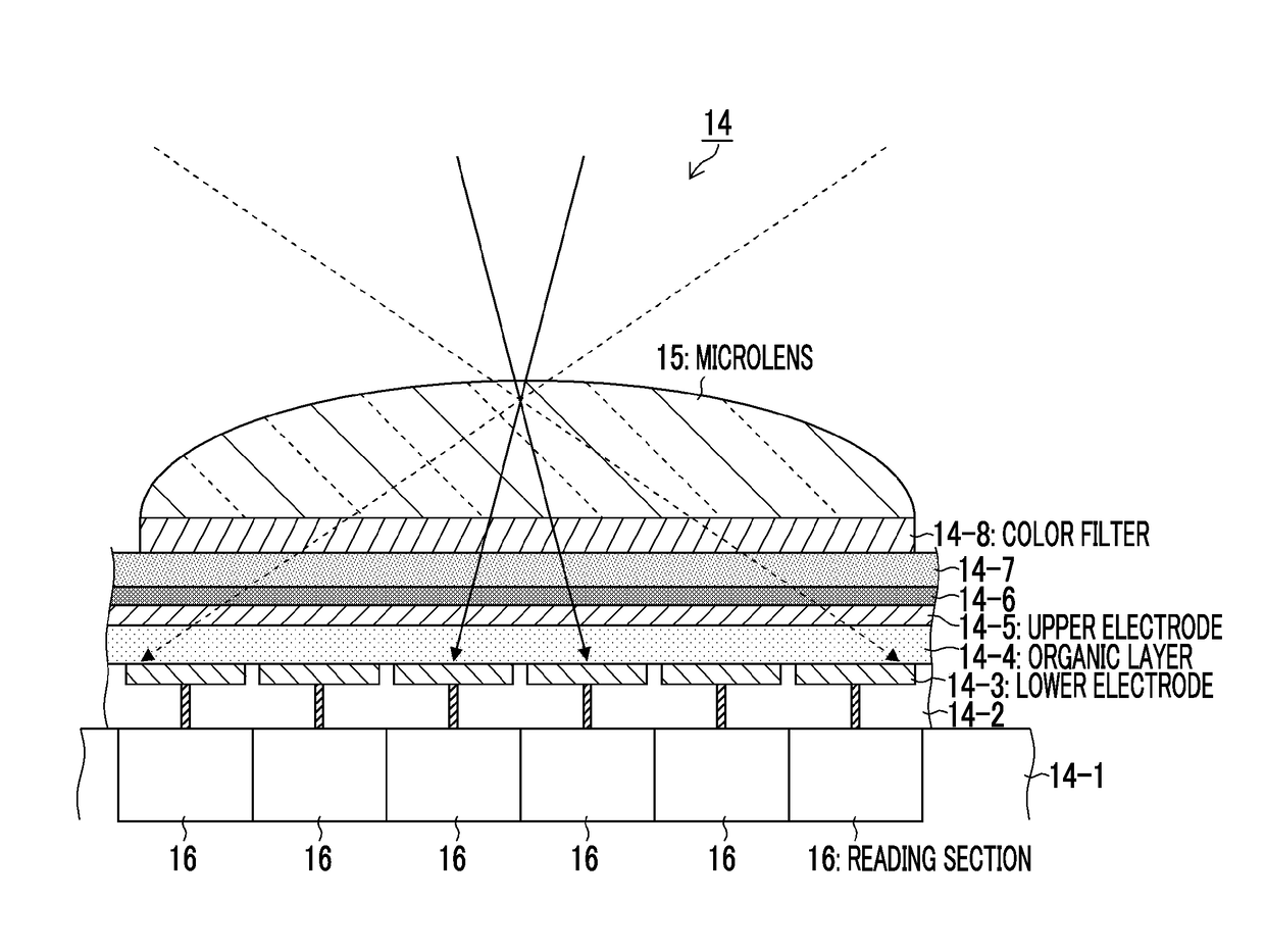
[0015]Further, according to the present aspect, the image sensor having the organic layer is used, and thus the photoelectric conversion section can be made to be thin. Thereby, in the present aspect, even in the pixel divided into the plurality of regions using the on-chip microlens, it is possible to acquire an image in which color mixture is minimized.
[0034]According to the present invention, the regions of the pixels divided by the electronic diaphragm section are selected, or the signals, which are read from the divided regions of the pixels, are selected, thereby generating an image on the basis of the signals. Accordingly, it is possible to acquire an image based on a desired aperture value even without a mechanical diaphragm. Furthermore, according to the present invention, the image sensor capable of reducing the thickness of the photoelectric conversion section is used, and thus it is possible to acquire an image in which color mixture is minimized.

Problems solved by technology

Hence, it is difficult for conventional cameras to obtain images based on a plurality of aperture values through a single exposure operation.

Method used


Image

  • Imaging device and imaging method
  • Imaging device and imaging method
  • Imaging device and imaging method

Examples


modification example 1

[0126]According to the present example, there are provided the divided regions which have smaller division widths in the center portion of the pixel than those in the peripheral portion of the pixel. Thereby, in the present example, there may be provided the divided regions based on dependency of the aperture value of a ray angle.

[0127]FIGS. 10A and 10B are schematic diagrams illustrating division of the pixel in Modification Example 1, in the pixel shown in FIGS. 7A and 7B. As shown in FIG. 10A, the separated electrodes 14-3 are divided with a small width in the central portion, and are divided with a larger width at a position closer to the peripheral portion. Further, as shown in FIG. 10B, when the pixel is viewed from the just above, the radii of the separated electrodes 14-3 are divided such that a plurality of different concentric circles overlaps with each other.

[0128]As shown in FIG. 10B, the divided region 111 corresponding to the aperture value F8 is a circle having a smal...

modification example 2

[0130]In the present example, there are provided divided regions which have different division widths in accordance with the color of the color filter 14-8. Thereby, it is possible to receive light by the divided regions which are quite appropriate even for light with long wavelengths.

[0131]FIGS. 11A to 11C are schematic diagrams illustrating change in division widths of the divided regions corresponding to the small-aperture-side aperture value in accordance with the color of the color filter 14-8.

[0132]As shown in FIG. 11A, in a pixel having a red color filter 120, a divided region 126 corresponding to the small-aperture-side aperture value is a circle having a radius R(R). Further, as shown in FIG. 11B, in a pixel having a green color filter 122, a divided region 128 corresponding to the small-aperture-side aperture value is a circle having a radius R(G). Furthermore, as shown in FIG. 11C, in a pixel having a blue color filter 124, a divided region 130 corresponding to the small-...

modification example 3

[0135]In the present example, in accordance with the position of the pixel in the image sensor 14, a method of dividing the separated electrodes 14-3 is changed. In the present example, so-called scaling in the image sensor 14 is performed. Thereby, light can be precisely received in the divided regions even in the central and peripheral portions of the image sensor 14.

[0136]FIG. 12 is a schematic diagram of a main lens 140 and the image sensor 14 provided in the photography optical system 12.

[0137]As shown in FIG. 12, the image sensor 14 is formed of a plurality of pixels. Further, for convenience of description, only necessary parts of the pixels of the image sensor 14 are shown, and the others are omitted.

[0138]Each of the pixels, which are disposed in the central portion of the image sensor 14, is divided in symmetric with respect to the center of the pixel. That is, in a sectional view of the separated electrodes 14-3 (refer to FIG. 4, FIG. 7A, FIG. 9A, or FIG. 10A), the separa...


PUM


Abstract

The imaging device 1 has an image sensor 14 and an electronic diaphragm section. In the image sensor 14, a plurality of pixels having an organic layer for photoelectric conversion is two-dimensionally arranged. Each pixel of the image sensor 14 is divided into a plurality of regions. The pixel has an on-chip microlens 15, which forms a pupil image of a photography optical system 12 on the plurality of regions, and reading sections 16 which respectively read photoelectrically converted signals of the divided regions. The electronic diaphragm section electronically controls an aperture value, and selects divided regions, which are read by the reading sections 16, on the basis of the aperture value, or selects a signal from the signals of the plurality of divided regions, which are read by the reading sections 16, on the basis of the aperture value.

Description

CROSS-REFERENCE TO RELATED APPLICATIONS[0001]This application is a Continuation of PCT International Application No. PCT / JP2014 / 074816 filed on Sep. 19, 2014, which claims priority under 35 U.S.C. §119(a) to Japanese Patent Application No. 2013-202083 filed on Sep. 27, 2013. Each of the above applications is hereby expressly incorporated by reference, in their entirety, into the present application.BACKGROUND OF THE INVENTION[0002]1. Field of the Invention[0003]The present invention relates to an imaging device and an imaging method. In particular, the present invention relates to an imaging device, which has an image sensor where an organic layer serves as a photoelectric conversion section, and an imaging method therefor.[0004]2. Description of the Related Art[0005]In conventional cameras having mechanical diaphragms, an aperture value (F number) used when the imaging element is exposed is fixed to a single value, and thus only an image according to the aperture value can be obtai...

Claims


Application Information

Patent Timeline
Patent Type & Authority Patents(United States)
IPC IPC(8): H04N5/238H04N5/225G03B7/26G02B3/00G03B9/02H04N9/04H04N5/235H01L27/30H04N5/374
CPCH04N5/238G02B3/0056G03B7/26G03B9/02H01L27/307H04N9/045H04N5/2254H04N5/2351H04N5/2353H04N5/374H01L27/14627H04N23/55H04N23/75H04N23/71H04N23/73H04N25/76H04N25/134H10K39/32
Inventor AOKI, TAKASHIOOTSUKI, YASUO
Owner FUJIFILM CORP
Learn More