
Chip manufacturing method and liquid ejecting head manufacturing method

a manufacturing method and liquid ejection technology, applied in the direction of piezoelectric/electrostrictive transducers, transducer types, printing, etc., can solve the problem that the edge of the reservoir side cannot provide a lead electrode, and achieve the effect of reducing the erosion of the flow path

Active Publication Date: 2016-06-28
SEIKO EPSON CORP
View PDF18 Cites 1 Cited by
  • Summary
  • Abstract
  • Description
  • Claims
  • Application Information

AI Technical Summary

Benefits of technology

The invention simplifies the process of manufacturing chips by using a laser beam to create fragile sections on the substrates, which can then be easily divided to separate the substrates. This is particularly useful in the manufacturing of liquid ejecting heads, where the process of dividing the substrates can be a time-consuming and costly step. The use of a vibrating plate and a metallic film on the substrate surface can improve the accuracy and reliability of the fragile section formation. Additionally, a protection film can be used to prevent damage to the substrate during the manufacturing process. The use of the same material as the metallic film can reduce manufacturing costs and ensure optimal thinness of the film. Overall, the invention simplifies the chip manufacturing process and reduces manufacturing costs.

Problems solved by technology

In addition, the edge of the reservoir side cannot provide a lead electrode for connecting the reservoir to a drive circuit of a piezoelectric element.
The above-described problems are similarly present in various methods of separating a first substrate and a second substrate bonded to each other into chips.

Method used


Image

  • Chip manufacturing method and liquid ejecting head manufacturing method
  • Chip manufacturing method and liquid ejecting head manufacturing method
  • Chip manufacturing method and liquid ejecting head manufacturing method

Examples


Embodiment Construction

[0033]Hereinafter, embodiments of the invention will be described. The embodiments described below merely exemplify the invention.

1. Example of Liquid Ejecting Head Obtained from Manufacturing Method of the Invention

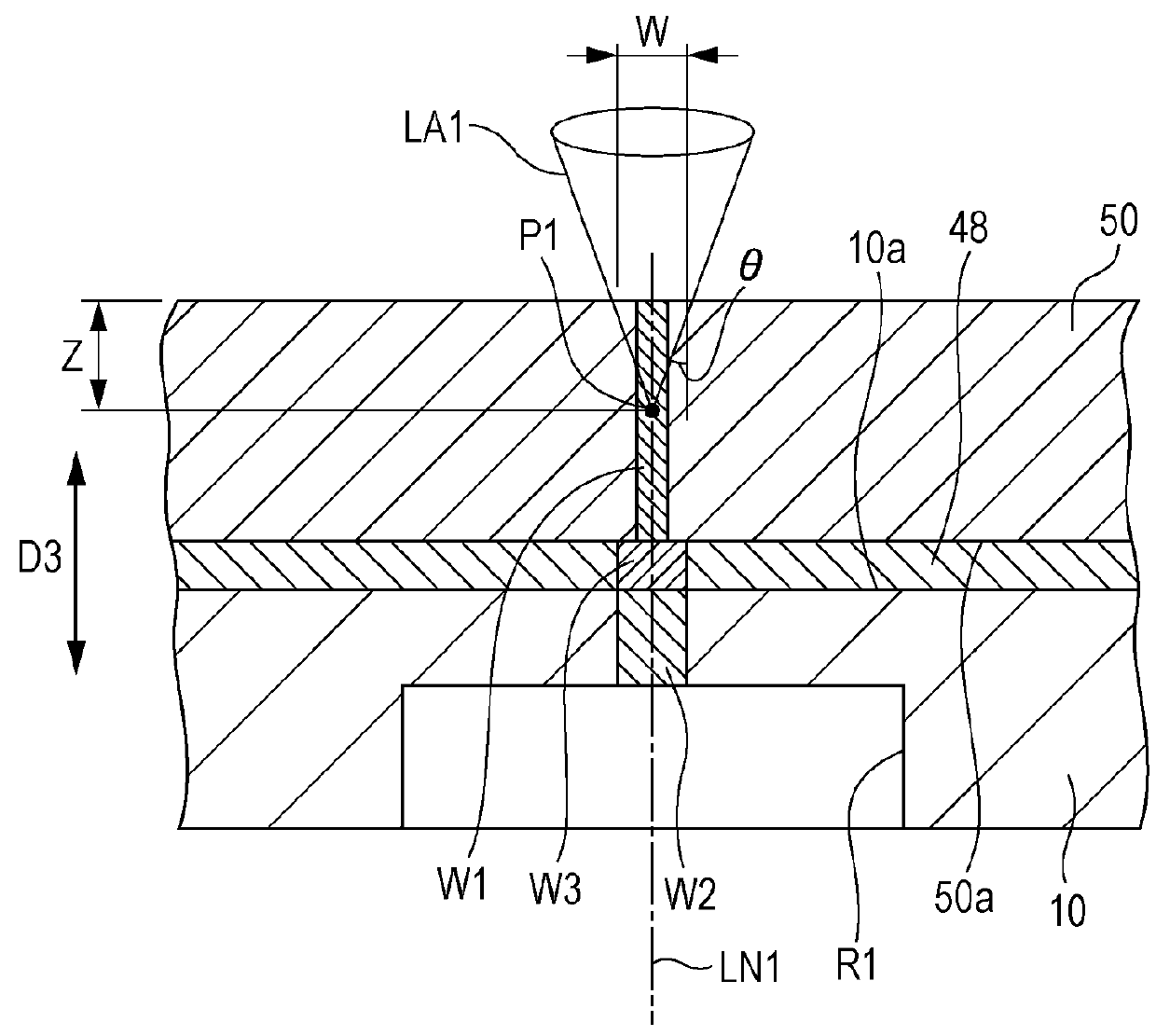
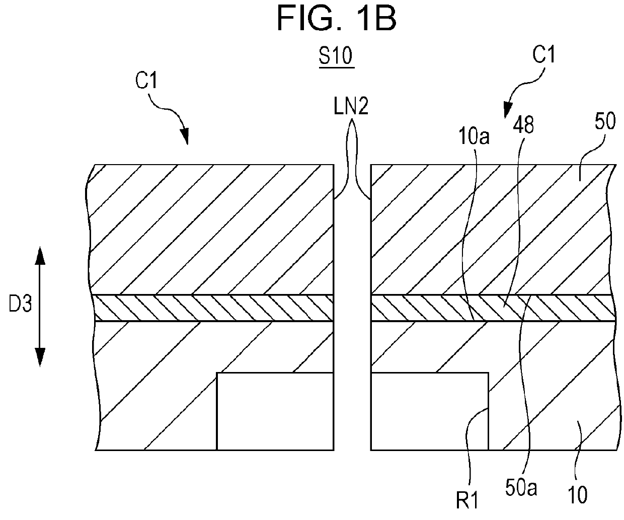
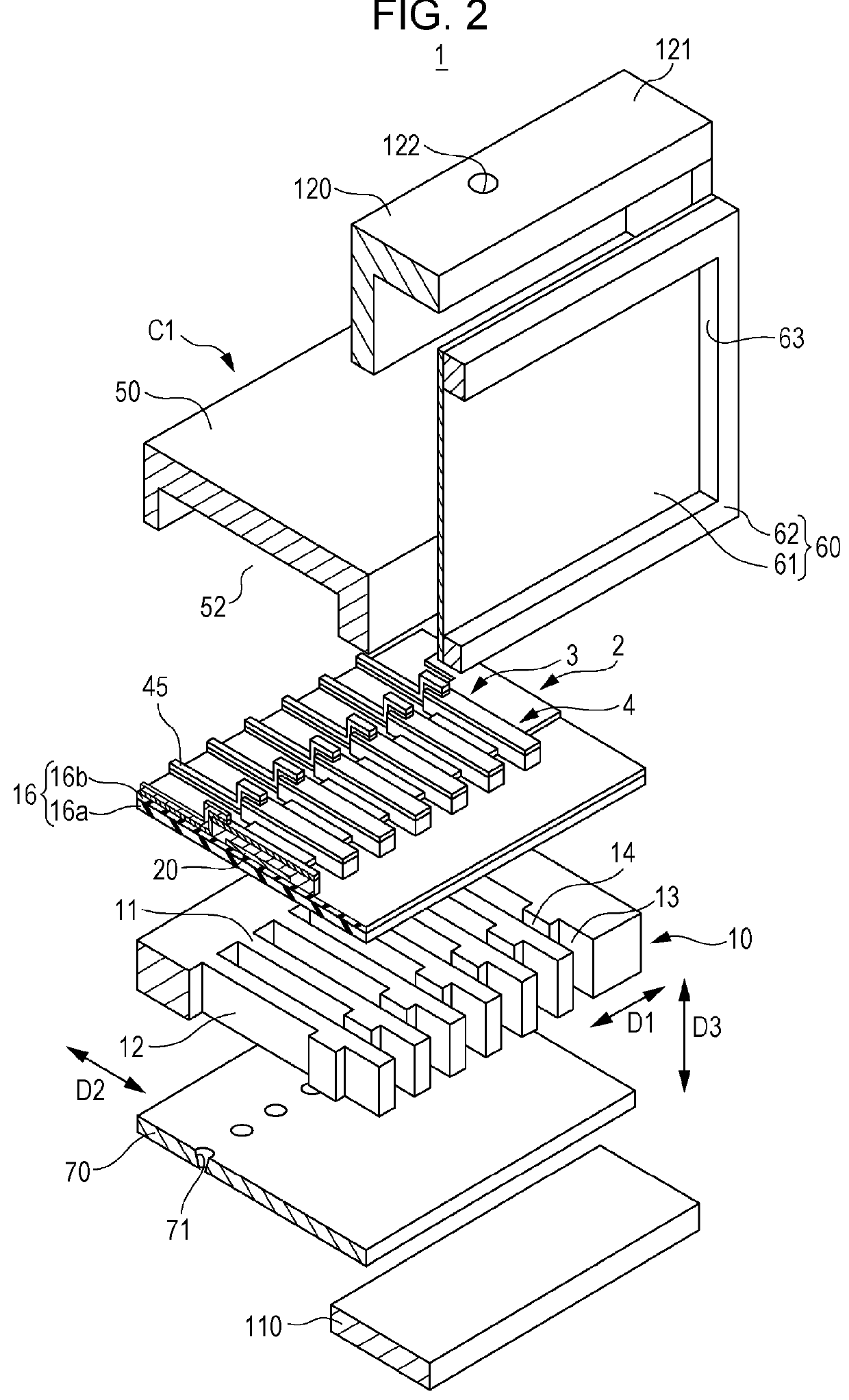
[0034]FIG. 1A is a vertical cross-sectional view schematically illustrating a state in which fragile sections (W1, W2) are formed with an irradiation of a laser beam LA1. FIG. 1B is a vertical cross-sectional view illustrating a state in which substrates (10, 50) are divided along the fragile sections (W1, W2). FIG. 2 is an exploded perspective view explodedly illustrating a main portion of a recording head 1 that is an example of a liquid ejecting head obtained from a manufacturing method of the invention for convenience. FIG. 3A is a plan view illustrating an outline of a configuration of the recording head 1. FIG. 3B is a vertical cross-sectional view in which one segment of the recording head 1 is broken at a position of IIIB-IIIB of FIG. 3A. A microstructure having ...


PUM

PropertyMeasurementUnit
thicknessaaaaaaaaaa
thicknessaaaaaaaaaa
thicknessaaaaaaaaaa

Abstract

A liquid ejection apparatus manufacturing method includes forming a metallic film in at least the section to be cut of a bonding surface between the flow path forming substrate (a second substrate) and the protection substrate (a first substrate); forming a first fragile section on the protection substrate by irradiating the section to be cut of the protection substrate bonded to the flow path forming substrate from the protection substrate side with a laser beam whose condensing point is focused thereon, and forming a second fragile section on the flow path forming substrate by melting the metallic film of the section to be cut; and dividing the protection substrate and the flow path forming substrate bonded to each other along the first fragile section and the second fragile section.

Description

BACKGROUND[0001]1. Technical Field[0002]The present invention relates to a chip manufacturing method of separating a first substrate and a second substrate bonded to each other into chips, a liquid ejecting head manufacturing method, and a liquid ejecting apparatus manufacturing method.[0003]2. Related Art[0004]As a liquid ejecting head used in an ink jet printer and the like, for example, an ink jet recording head that is obtaining by laminating a nozzle plate having an nozzle opening, a flow path forming substrate provided with a vibrating plate or a piezoelectric element and a reservoir forming substrate has been known. JP-A-2008-119905 discloses a manufacturing method of dividing the flow path forming substrate and the reservoir forming substrate bonded to each other into a plurality of silicon devices with a laser beam. The manufacturing method discloses forming an elastic film made of silicon dioxide on a silicon substrate, forming an insulator film made of zirconium oxide on ...

Claims


Application Information

Patent Timeline
Patent Type & Authority Patents(United States)
IPC IPC(8): B21D53/76B41J2/16B23P17/00B41J2/045
CPCB41J2/1635B41J2/0451B41J2/0455B41J2/04541B41J2/04581B41J2/161B41J2/1629B41J2/1632B41J2/1645B41J2/1646Y10T29/42B41J2002/14241B41J2002/14419
Inventor MATSUMOTO, YASUYUKI
Owner SEIKO EPSON CORP
Learn More