Concurrent design process

a design process and concurrent technology, applied in the field of electronic design automation (eda), can solve the problems of extremely complex and involved designs, and the configuration of eda tools may be difficult to achiev

Active Publication Date: 2017-06-20
CADENCE DESIGN SYST INC
View PDF7 Cites 6 Cited by
  • Summary
  • Abstract
  • Description
  • Claims
  • Application Information

AI Technical Summary

Problems solved by technology

Some EDA tools may be configured to operate upon extremely complex and involved designs that may require the attention of multiple designers each of whom may be physically located in different areas throughout the world.

Method used


Image

  • Concurrent design process
  • Concurrent design process
  • Concurrent design process

Examples


Embodiment Construction

[0045]Reference will now be made in detail to the embodiments of the present disclosure, examples of which are illustrated in the accompanying drawings. The present disclosure may, however, be embodied in many different forms and should not be construed as being limited to the embodiments set forth herein. Rather, these embodiments are provided so that this disclosure will be thorough and complete, and will fully convey the concept of the disclosure to those skilled in the art.

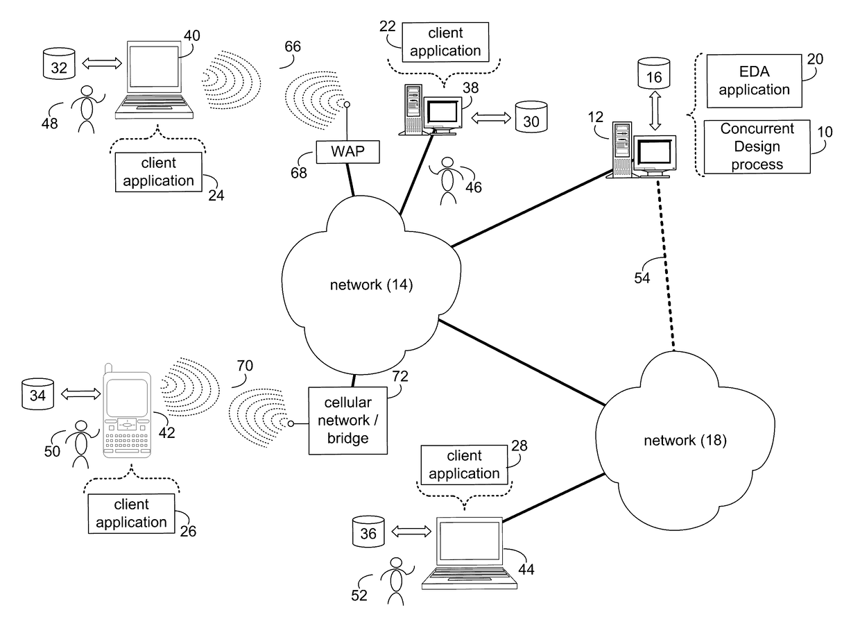
[0046]Embodiments of the concurrent design process described herein may utilize one or more electronic design automation techniques and / or tools such as those available from the Assignee of the subject application. Embodiments of concurrent design process may provide a multi-user environment that may allow for the creation of a layout of an electronic circuit design such as a printed circuit board (“PCB”). Accordingly, multiple users may be able to simultaneously work on a PCB / Package Design using the same com...


PUM


Abstract

The present disclosure relates to a method for multi-user, at least partially concurrent, electronic circuit design. Embodiments may include receiving, at a client computing device, a user input corresponding to a change to an electronic circuit design, wherein the electronic circuit design is accessible by multiple users in an at least partially concurrent manner. Embodiments may also include implementing the change to the electronic circuit design at the client computing device without receiving authorization from a server computing device and transmitting the implemented change to the electronic circuit design to the server computing device.

Description

FIELD OF THE INVENTION[0001]The present disclosure relates to electronic design automation (EDA), and more specifically, to a method for allowing multiple users, who may be geographically dispersed, to operate on and / or edit an electronic design.DISCUSSION OF THE RELATED ART[0002]EDA utilizes software tools that may be used in the design and analysis of numerous electronic systems such as printed circuit boards (PCBs) and integrated circuits (ICs). Recent years have seen unprecedented expansion of functional requirements for PCB designs. Some EDA tools may be configured to operate upon extremely complex and involved designs that may require the attention of multiple designers each of whom may be physically located in different areas throughout the world.SUMMARY OF INVENTION[0003]In one or more embodiments of the present disclosure, a computer-implemented method for multi-user, at least partially concurrent, electronic circuit design is provided. The method may include receiving, at ...

Claims


Application Information

Patent Timeline
Patent Type & Authority Patents(United States)
IPC IPC(8): G06F17/50
CPCG06F17/5045G06F17/5072G06F2111/02G06F30/30
Inventor BERNARD, PATRICKBUZZELL, GEORGE MALCOLMBERGAN, SEANFARMAR, FRANK X.
Owner CADENCE DESIGN SYST INC
Why Eureka
Try Eureka