Optical element, image display device and method for manufacturing same

a technology of image display device and optical element, which is applied in the field of optical element, can solve the problems of film degradation risk, difficulty in achieving flatness and a mirror surface on the front and rear surfaces of light guide plates, etc., and achieves the effect of high flatness accuracy

Active Publication Date: 2017-08-22
SEIKO EPSON CORP
View PDF16 Cites 7 Cited by
  • Summary
  • Abstract
  • Description
  • Claims
  • Application Information

AI Technical Summary

Benefits of technology

[0006]In view of the above circumstances, an advantage of some aspects of the invention is that an optical element that has high accuracy in flatness on front and rear surfaces thereof and is free from film degradation and inclusion of foreign substances or air bubbles even in a case where a light guide plate having a multilayer structure is used, a method for manufacturing the optical element, and an optical device are provided.
[0012]The first or second aspect of the optical element according to the invention is preferably arranged such that the light guide plate includes a third part made of a light transmissive material and a second transflective layer disposed between the second part and the third part; the second transflective layer is disposed so as to be parallel with the first transflective layer; the second transflective layer reflects, toward the first surface side, at least part of light entering from the third part side and transmits the other part of the light entering from the third part side; and the first transflective layer reflects, toward the first surface side, at least part of light that has passed through the second transflective layer and entered from the second part side. In this case, light entering from the third part side travels toward the second part side while being reflected toward the first surface side by the second transflective layer, and is reflected by the first transflective layer toward the first surface side. That is, the incident light is emitted toward the first surface side while being guided. This makes it possible to display a large virtual image to a viewer.
[0013]The first or second aspect of the optical element according to the invention is preferably arranged such that reflectance of the first transflective layer on the second part side is higher than that of the second transflective layer on the third part side. In this case, even in a case where the optical path length is long, it is possible to avoid occurrence of brightness unevenness.
[0014]The first or second aspect of the optical element according to the invention is preferably arranged such that a perpendicular line from an end of the first transflective layer on the second surface side to the first surface intersects, on the first surface, with an end of the second transflective layer on the first surface side. In this case, the light exit surface has no region where reflected light does not reach. It is therefore possible to prevent occurrence of black stripes.
[0017]The first or second aspect of the optical element according to the invention is preferably arranged to further include: a light transmissive introduction block that introduces light into the light guide plate; and a mirror that reflects light toward the introduction block. In this case, light is introduced into the light guide plate by the mirror and the introduction block, and the light that has entered the light guide plate is reflected while being guided. This makes it possible to display a large virtual image to a viewer.

Problems solved by technology

However, in the case of manufacturing a light guide plate having a multilayer structure, it is difficult to achieve accuracy in flatness and a mirror surface on the front and rear surfaces of the light guide plate.
Furthermore, in the case of a multilayer structure, the transflective layer is exposed, and therefore there is a risk of film degradation.

Method used


Image

  • Optical element, image display device and method for manufacturing same
  • Optical element, image display device and method for manufacturing same
  • Optical element, image display device and method for manufacturing same

Examples


first embodiment

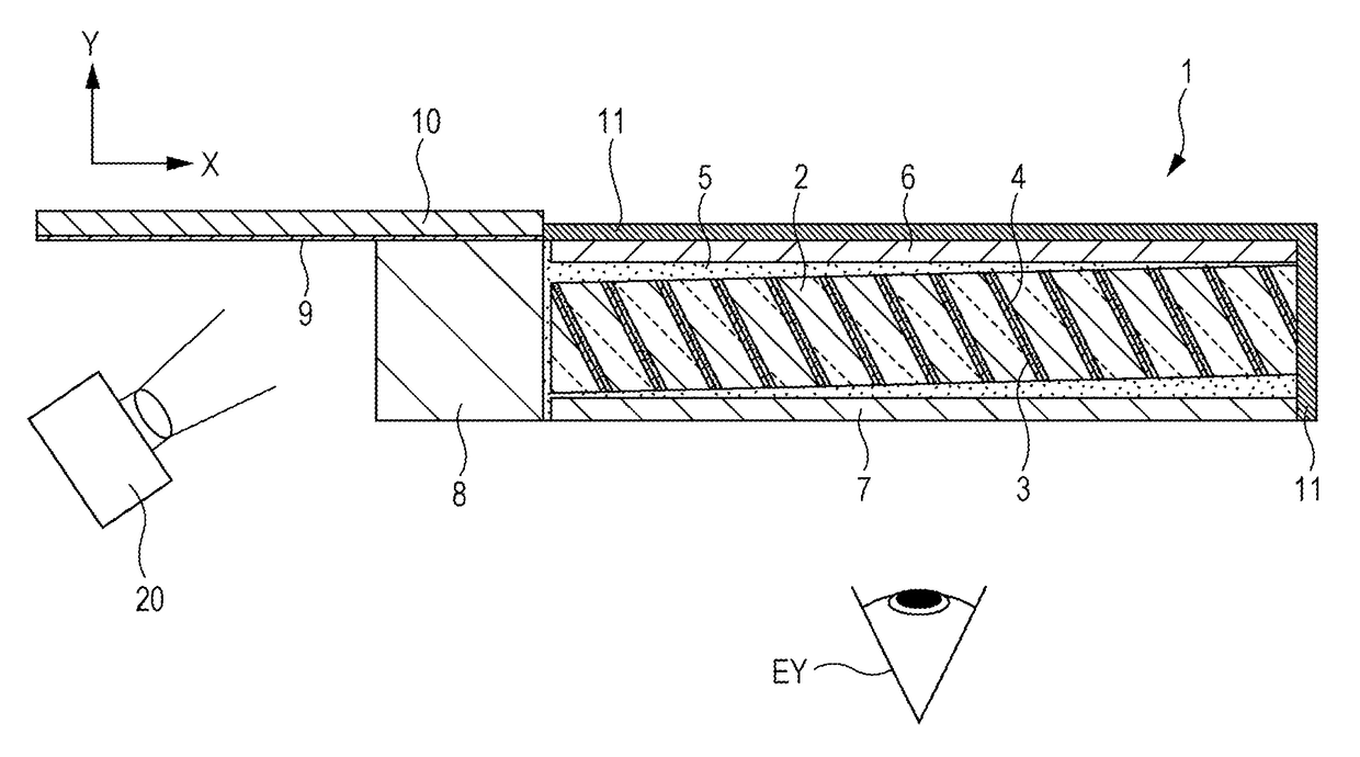
[0031]FIG. 1 is a side view illustrating the whole image of an optical device 1 according to the first embodiment. As illustrated in FIG. 1, the optical device 1 includes a light guide plate 2, an upper flat plate 6, a lower flat plate 7, an introduction block 8, an incident light intake mirror 9, and a mirror supporting plate 10.

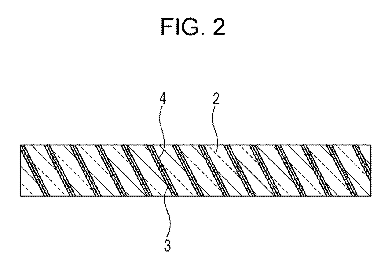
[0032]As illustrated in FIG. 2, the light guide plate 2 is created by (i) forming a transflective layer 3 on plate-like members made of a material such as a light transmissive resin material by a method such as vapor deposition, (ii) bonding, with an adhesive 4, such plate-like members on which the transflective layer 3 has been formed so that the plate-like members are shifted from each other in accordance with an inclination angle, and (iii) cutting the plate-like members thus bonded.

[0033]The light guide plate 2 is bonded to the upper flat plate 6 and the lower flat plate 7 with an adhesive 5, and the upper flat plate 6 and the lower flat plate 7 are kep...

second embodiment

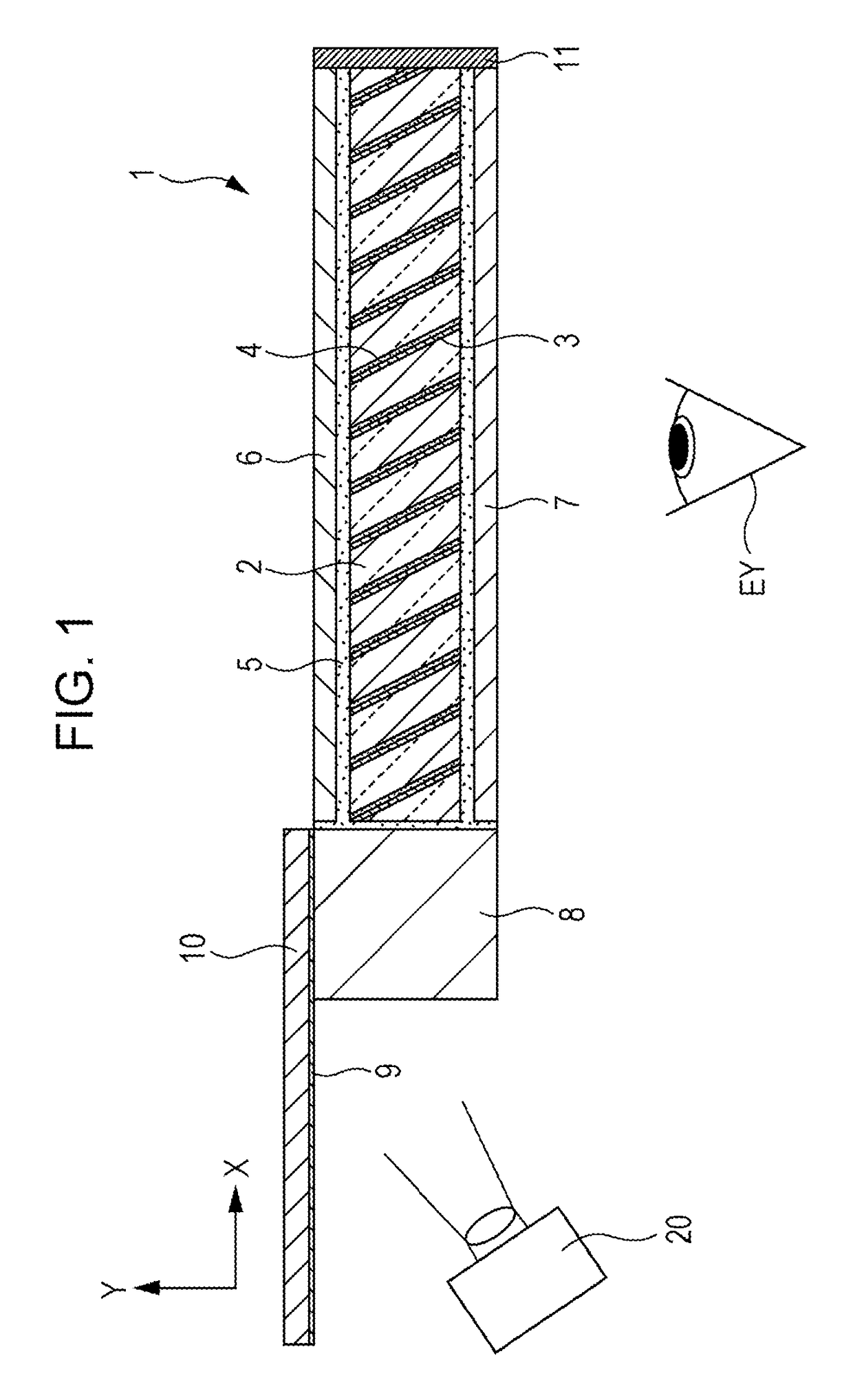
[0046]The second embodiment of the invention is described with reference to FIG. 3. As illustrated in FIG. 3, a light guide plate 2 may be bonded in an inclined state to an upper flat plate 6 and a lower flat plate 7. Even in such a case where the light guide plate 2 is inclined, a gap between the upper flat plate 6 and the light guide plate 2 and a gap between the lower flat plate 7 and the light guide plate 2 are filled with an adhesive 5, and therefore flatness of a topmost surface of the upper flat plate 6 and a bottommost surface of the lower flat plate 7 can be achieved and the topmost surface of the upper flat plate 6 and the bottommost surface of the lower flat plate 7 can be kept parallel with each other. Also in the present embodiment, surface roughness of the top surface and the bottom surface of the light guide plate 2 itself can be covered by the adhesive 5, and the parallelism of the top surface and the bottom surface can be secured by the upper flat plate 6 and the lo...

third embodiment

[0048]The third embodiment of the invention is described with reference to FIGS. 4 and 5. In the first embodiment and the second embodiment, an example in which an upper flat plate 6 and a lower flat plate 7 are bonded to a light guide plate 2 with an adhesive 5 has been described. However, the invention is not limited to this example.

[0049]For example, it is possible that a light guide plate 2 be placed in a mold 30 whose top and bottom surfaces are kept parallel with each other and whose left and right surfaces are kept parallel with each other and the mold 30 be filled with an adhesive 5 or a resin as illustrated in FIG. 4. The light guide plate 2 that has been unified with the adhesive 5 or the resin can be obtained by removing the mold 30 as illustrated in FIG. 5 after the adhesive 5 or the resin is cured. In this case, flatness and parallelism of a top surface and a bottom surface of the adhesive 5 or the resin can be kept. It should be noted that the flatness just needs to be...


PUM

PropertyMeasurementUnit
refractive indexaaaaaaaaaa
reflectanceaaaaaaaaaa

Abstract

An optical element includes a light guide plate that has therein a light transmissive flat plate member on which a transflective layer is formed, and a layer of a light transmissive adhesive or a light transmissive resin layer that uniformly covers the light guide plate. The refractive index of the layer of the adhesive or the resin layer is set to a refractive index different from that of the light guide plate. A first surface of the layer of the adhesive or the resin layer that is on the light exit surface side of the light guide plate is kept parallel with a second surface of the layer of the adhesive or the resin layer that is on the opposite side to the light exit surface side of the light guide plate.

Description

BACKGROUND[0001]1. Technical Field[0002]The present invention relates to an optical element such as a light guide plate, an image display device, and a method for manufacturing the optical element and the image display device.[0003]2. Related Art[0004]A virtual image display has a light source and a transmission type display element (e.g., LCD, OLED) that transmits light emitted from the light source. JP-T-2003-536102 proposes a virtual image display device that includes a light source emitting, as light including information, display light and a light guide plate disposed so as to reflect or diffract, toward a viewer, the light including the information so that a virtual image formed by the light guide plate is viewable in the front of the viewer.[0005]According to JP-T-2003-536102, for example, a light guide plate having a multilayer structure is used as a light guide plate including a transflective layer. However, in the case of manufacturing a light guide plate having a multilay...

Claims


Application Information

Patent Timeline
Patent Type & Authority Patents(United States)
IPC IPC(8): G02B27/14B29D11/00G02B27/01F21V8/00
CPCB29D11/00663G02B6/005G02B27/0172G02B6/0046G02B6/0055G02B2027/013G02B2027/0178G02B6/0031G02B6/0065G02B2027/0125
Inventor TATSUGI, HIROYUKI
Owner SEIKO EPSON CORP
Why Eureka
Try Eureka