Light-emitting device with alternating arrangement of anode pads and cathode pads

a light-emitting device and cathode pad technology, applied in the direction of semiconductor devices, organic semiconductor devices, electrical devices, etc., can solve the problems of reducing assembly efforts for light-emitting devices having an improved degree of homogeneity of light emission, and achieve the effect of reducing assembly efforts, improving the degree of homogeneity of light emission, and reducing assembly efforts

Active Publication Date: 2017-08-29
OLEDWORKS GMBH
View PDF35 Cites 0 Cited by
  • Summary
  • Abstract
  • Description
  • Claims
  • Application Information

AI Technical Summary

Benefits of technology

[0004]It is an object of the present invention to provide a light-emitting device, particularly an OLED, which has an improved degree of homogeneity of light emission and which can be assembled with reduced efforts. It is a further object of the present invention to provide a production method for producing the light-emitting device with reduced assembly efforts, and to a production apparatus for performing the production method.
[0006]The alternating arrangement of anode and cathode pads results in a more homogenous electrical field between the anode and the cathode and therefore allows for an improved degree of homogeneity of light emission. And because the alternating arrangement of anode and cathode pads, the encapsulation, the anode electric connector and the cathode electrical connector are configured such that the anode pads are electrically connected by a straight part of the anode electrical connector and the cathode pads are electrically connected by a straight part of the cathode electrical connector, the electrical contacting procedure for electrically contacting the anode and cathode pads can be performed relatively easily by just providing the straight parts of the anode electrical connector and the cathode electrical connector on the part of the encapsulation that has the openings. For instance, the electrical connection of the anode and cathode pads can be provided by just depositing two straight metal stripes resulting in reduced assembly efforts for a light-emitting device having an improved degree of homogeneity of light emission.
[0009]The alternating arrangement of anode and cathode pads, the encapsulation, the anode electrical connector and the cathode electrical connector may be configured such that the encapsulation electrically insulates the anode pads from the straight part of the cathode electrical connector and electrically insulates the cathode pads from the straight part of the anode electrical connector. Since the encapsulation is also used for electrically insulating the anode pads from the cathode electrical conductor and the cathode pads from the anode electrical conductor, an additional means like an additional layer may not be needed for providing this electrical insulation, thereby further reducing the assembly efforts.
[0010]The light emission source may comprise several sides, and the alternating arrangement of anode and cathode pads may be located at one side of the light emission source only. It has been found that locating the alternating arrangement at one side of the light emission source only can be sufficient for providing a relatively homogeneous emission of the light such that it may not be necessary to provide the alternating arrangement at two or more sides of the light emission source. This can further reduce the assembly efforts.
[0011]An insulator may be arranged in regions connecting the anode pads with the anode for electrically insulating these regions from the cathode. An insulator may be arranged in each of these regions. This can simplify deposition of the cathode such that the cathode does not contact the anode and the anode pads.

Problems solved by technology

For instance, the electrical connection of the anode and cathode pads can be provided by just depositing two straight metal stripes resulting in reduced assembly efforts for a light-emitting device having an improved degree of homogeneity of light emission.

Method used


Image

  • Light-emitting device with alternating arrangement of anode pads and cathode pads
  • Light-emitting device with alternating arrangement of anode pads and cathode pads
  • Light-emitting device with alternating arrangement of anode pads and cathode pads

Examples


Embodiment Construction

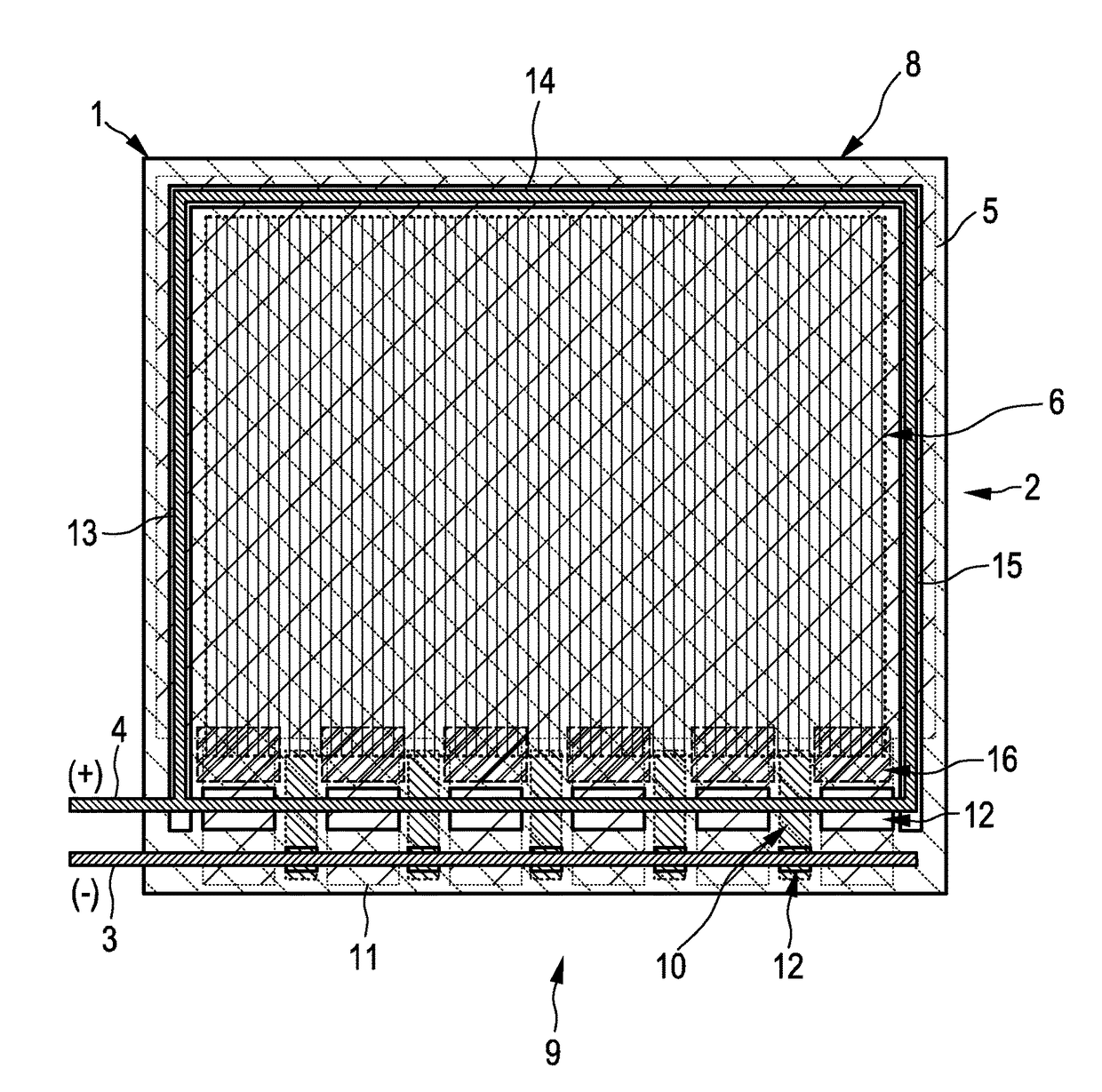
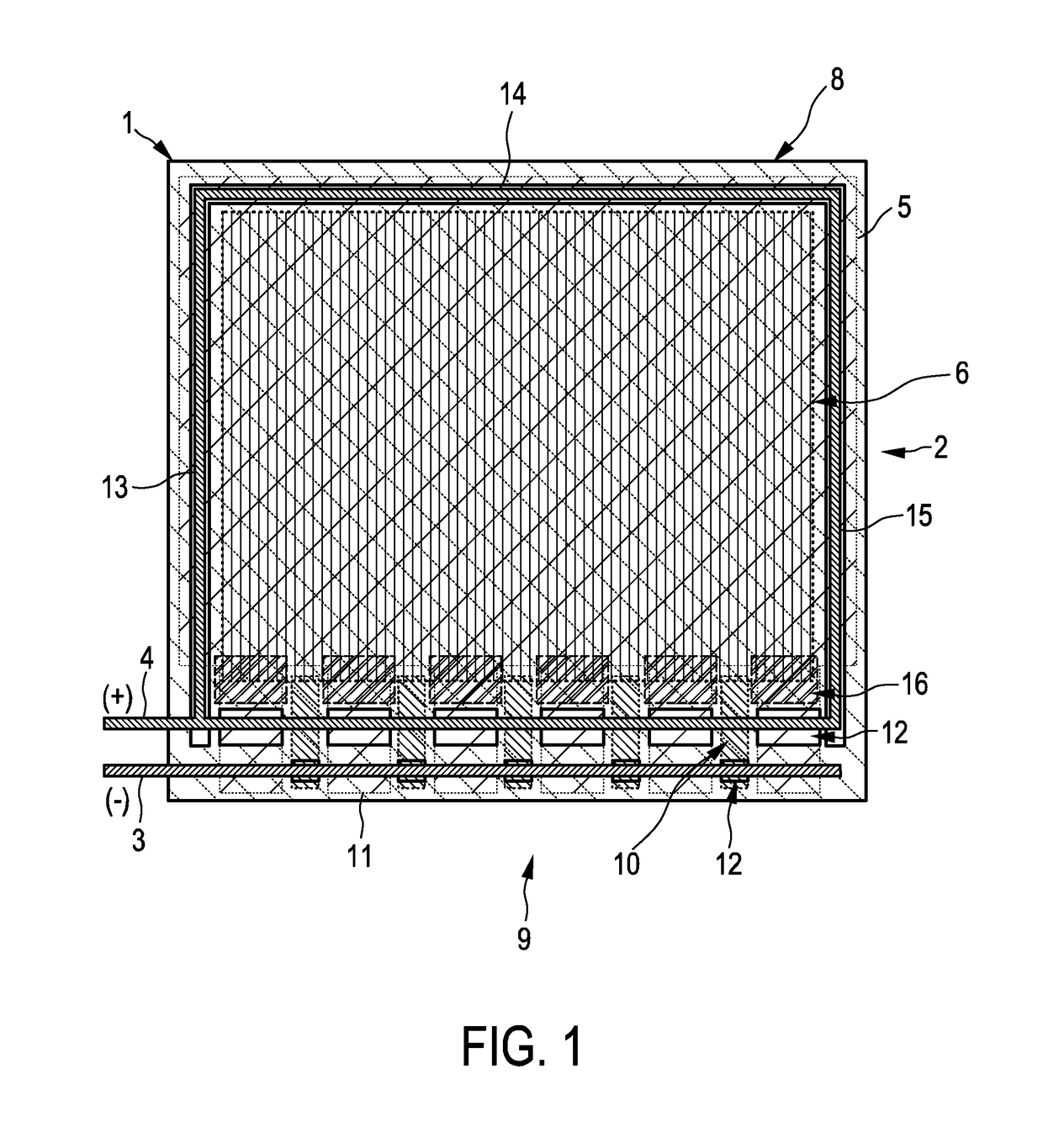
[0027]FIG. 1 shows schematically and exemplarily an embodiment of a light-emitting device being an OLED. The OLED 1 comprises a light emission source 2 comprising an anode 5, a cathode 6, a light emission region between the anode 5 and the cathode 6 and an alternating arrangement 9 of anode pads 11 for electrically connecting the anode 5 and cathode pads 10 for electrically connecting the cathode 6. The light emission region is adapted to emit light, if a voltage is applied between the anode 5 and the cathode 6. An insulator 16 is arranged in regions connecting the anode pads 11 with the anode 5, in order to electrically insulate these regions from the cathode 6.

[0028]The light emission source 2 of the OLED 1 is located between a substrate (not explicitly shown in FIG. 1) and a thin-film encapsulation (TFE) 8 that encapsulates the light emission source 2. The alternating arrangement 9 of anode and cathode pads 10, 11 is supported by the substrate, and the TFE 8 comprises openings 12...


PUM


Abstract

The invention relates to a light-emitting device like an OLED comprising a light emission region between an anode (5) and a cathode (6). An alternating arrangement (9) of anode pads (11) for electrically connecting the anode and cathode pads (10) for electrically connecting the cathode and an encapsulation (8) are configured such that the anode and cathode pads are electrically connectable by straight anode and cathode electrical connectors (3, 4) through openings (12) of the encapsulation. The alternating arrangement of the anode and cathode pads can lead to a more homogenous electrical field between the anode and the cathode and therefore allows for an improved degree of homogeneity of light emission. More, since the alternating arrangement of the anode and cathode pads is connectable by corresponding straight connectors, the contacting of the pads can be performed technically relatively easily.

Description

CROSS-REFERENCE TO PRIOR APPLICATIONS[0001]This application is the U.S. National Phase application under 35 U.S.C. §371 of International Application No. PCT / EP2014 / 060537, filed on May 22, 2014, which claims the benefit of European Patent Application No. 13168856.6, filed on May 23, 2013. These applications are hereby incorporated by reference herein.FIELD OF THE INVENTION[0002]The invention relates to a light-emitting device, in particular, to an organic light-emitting device (OLED). The invention also relates to a production method for producing the light-emitting device, and to a production apparatus for performing the production method.BACKGROUND OF THE INVENTION[0003]An OLED comprises an anode, a cathode and a light emission region between the anode and the cathode, wherein the light emission region is adapted to emit light, if a voltage is applied between the anode and the cathode. In operation, OLEDs may have an inhomogeneous electrical field between the anode and the cathode...

Claims


Application Information

Patent Timeline
Patent Type & Authority Patents(United States)
IPC IPC(8): H01L33/36H01L51/52H01L51/00H01L51/56
CPCH01L51/5203H01L51/0021H01L51/5253H01L51/56H01L2251/5361H10K50/805H10K50/844H10K71/00H10K71/60
Inventor RICKERS, CHRISTOPH
Owner OLEDWORKS GMBH
Why Eureka
Try Eureka