Laser Printing System

a laser array and laser printing technology, applied in semiconductor lasers, additive manufacturing processes, instruments, etc., can solve the problems of reliability and service costs of such addressable arrays, and achieve the effects of reducing the alignment effort of laser arrays, improving the homogeneity of total intensity distribution, and manufacturing costs

Active Publication Date: 2016-09-29
EOS ELECTRO OPTICAL SYST
View PDF4 Cites 75 Cited by
  • Summary
  • Abstract
  • Description
  • Claims
  • Application Information

AI Technical Summary

Benefits of technology

[0019]The laser arrays of each laser module may alternatively be arranged in an elongated arrangement with the long side of the elongated arrangement being arranged slanted or rotated with respect to the direction being perpendicular to the direction of movement of the object in the working plane. A defined slanting angle or rotation of the elongated arrangement of laser modules around their centers may enable integrated intensity profiles with smooth slopes, which may also overlap with the adjacent pixels, to improve the homogeneity of the total intensity distribution, especially if the pixels are slightly misaligned with respect to each other. The latter reduces the alignment effort of the laser arrays and thus the manufacturing costs of the laser modules and the laser printing system. The misalignment may in extreme cases be compensated by an additional calibration run of the laser printing system in which the velocity of movement of the object in relation to the energy input per time and area element of a calibration object is determined.
[0020]Alternatively, two, three or more laser arrays of the same laser module or different laser modules may be arranged to illuminate the same area element of the object. The laser arrays may be arranged to subsequently illuminate the area element. The energy input per time to an area element of the object in the working plane may be increased. This may enable higher velocities of the object and thus higher throughput of the laser printing system. Furthermore, the tolerance regarding misalignment of laser arrays and malfunctions of single semiconductor lasers may be improved. The driving schemes of different arrays may be adapted based on calibration runs with calibration objects as described above.
[0021]The optical element of the laser modules may be arranged to demagnify the image of the laser arrays in the working plane. The demagnification may enable a smaller pixel size and higher energy densities. Each laser array may further comprise a micro-lens array being part of the optical element, the micro-lens array may be arranged to lower the divergence of the laser light emitted by the semiconductor lasers. The reduction of the divergence may be used to find a compromise between an overlap of the laser light emitted by the semiconductor lasers in the object plane and the size of the single pixel. Furthermore, the distance between the laser array and the working plane may be adapted by means of the micro-lens array and / or the optical element (imaging optic) may be simplified.
[0022]The density of laser arrays may change in dependence of an area of the object to be illuminated by means of the laser printing system. The latter may enable higher power densities at defined parts of the object. Alternatively or in addition the density of the semiconductor lasers within the arrays may be adapted such that, for example, less or more intensity may be provided at the rim of the pixels. Furthermore, the shape of the arrays may be tailored in order to improve the homogeneity and / or to create a defined intensity distribution in the working plane. The arrays may, for example, have a diamond, triangle, round, elliptical, trapezoid or parallelogram shape.

Problems solved by technology

Reliability and service costs of such addressable arrays may be an issue.

Method used


Image

  • Laser Printing System
  • Laser Printing System
  • Laser Printing System

Examples


Embodiment Construction

[0082]Various embodiments of the invention will now be described by means of the Figures.

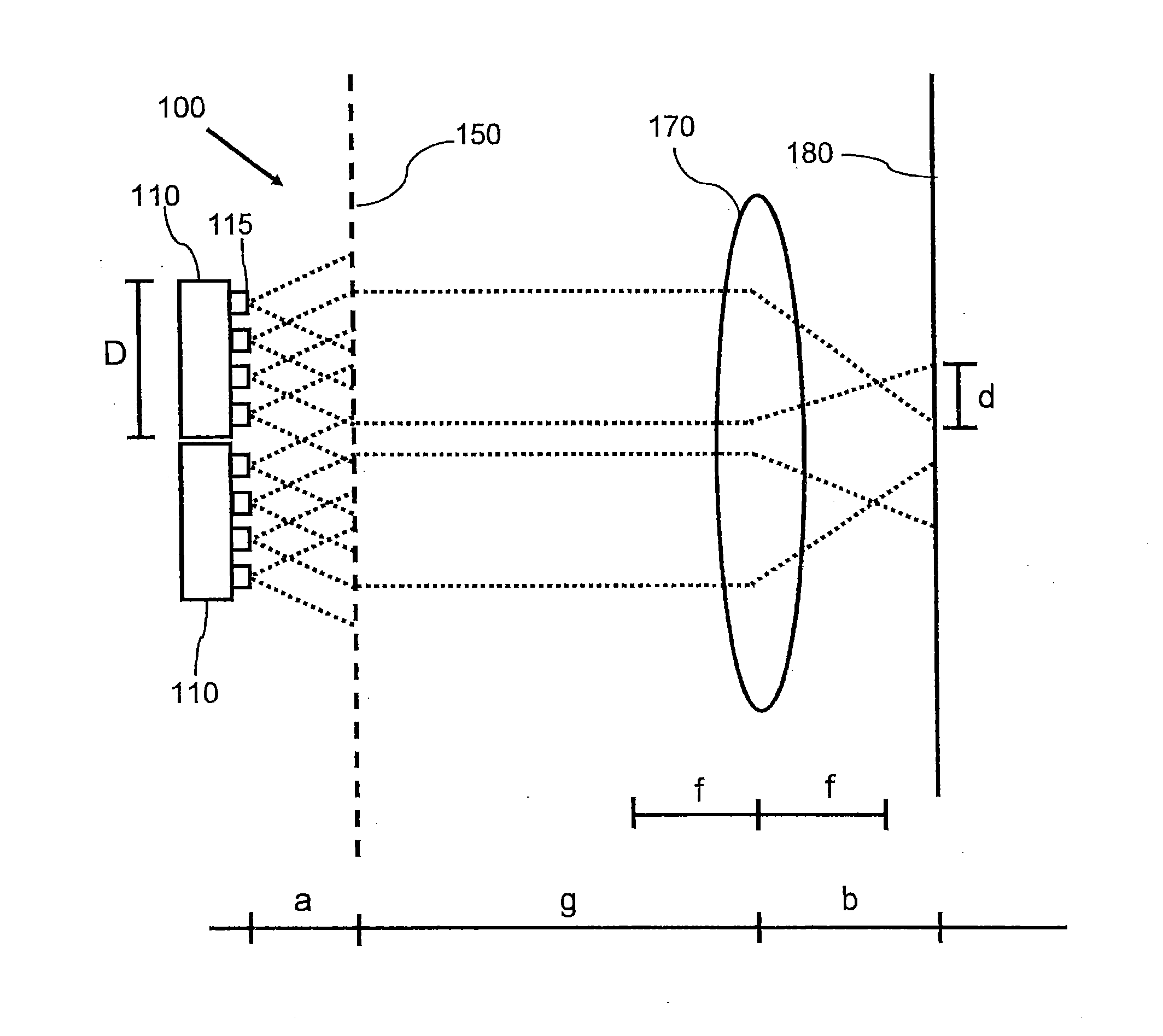
[0083]FIG. 1 shows a principal sketch of a first laser printing system 100. The laser printing system 100 comprises two laser arrays 110 with semiconductor lasers 115 and an optical element 170. The semiconductor lasers 115 are VCSELs which are provided on a semiconductor chip. In this case all VCSELs 115 of one array 110 are provided on one chip. The optical element 170 is an imaging lens with a focal distance f. The arrays 110 have a width D perpendicular to the plane of the drawings which is diffusely imaged to a working plane 180 by means of the imaging lens. The width d of the diffuse image of each array 110 with the width D in the working plane 180 defines the width of a pixel in the working plane 180. The width of the pixels d is smaller than the width D of the respective array. The images of the arrays are thus demagnified. The distance b between the working plane 180 and the imaging len...


PUM

PropertyMeasurementUnit
areaaaaaaaaaaa
distanceaaaaaaaaaa
total energyaaaaaaaaaa

Abstract

The invention describes a laser printing system (100) for illuminating an object moving relative to a laser module of the laser printing system (100) in a working plane (180), the laser module comprising at least two laser arrays of semiconductor lasers and at least one optical element, wherein the optical element is adapted to image laser light emitted by the laser arrays, such that laser light of semiconductor lasers of one laser array is imaged to one pixel in the working plane of the laser printing system, and wherein the laser printing system is a 3D printing system for additive manufacturing and wherein two, three, four or a multitude of laser modules (201, 202) are provided, which are arranged in columns (c1, c2) perpendicular to a direction of movement (250) of the object in the working plane (180), and wherein the columns are staggered with respect to each other such that a first laser module (201) of a first column of laser modules (c1) is adapted to illuminate a first area (y1) of the object and a second laser module (202) of a second column (c2) of laser modules is adapted to illuminate a second area (y2) of the object, wherein the first area (y1) is adjacent to the second area (y2) such that continuous illumination of the object is enabled.

Description

FIELD OF THE INVENTION[0001]The invention relates to a laser printing system and a method of laser printing, namely in the field of 3D printing by means of lasers for additive manufacturing, for example, used for rapid prototyping. The invention does not refer to 2D printing such as printing of documents.BACKGROUND OF THE INVENTION[0002]Selective-laser melting machines consist of a single high-power laser and a scanner to scan the laser over the area to be illuminated. In such machines the laser and the scanner are arranged outside of a process chamber and the laserlight can pass through an entrance window into the process chamber that contains a building area. To increase the processing speed, it is desirable to have a printing head with several independent channels i.e. an addressable array of lasers covering a significant part of the area. Preferably, the printing head covers the full width of the area to be printed with one addressable laser source per pixel, so that the print h...

Claims


Application Information

Patent Timeline
Patent Type & Authority Applications(United States)
IPC IPC(8): B22F3/105B33Y10/00B33Y30/00B23K26/064B33Y50/02B23K26/342B23K26/08B29C67/00B33Y40/00
CPCB22F3/1055B29C67/0077B29C67/0085B29C67/0088B33Y10/00B22F2003/1057B33Y40/00B33Y50/02B23K26/342B23K26/0853B23K26/064B33Y30/00B41J2/451G03G15/225B29C64/153B29C64/277B29C64/282B29C64/268B29C64/393B22F10/28B22F12/44B22F12/45G02B3/0006H01S5/0071H01S5/423B41J2/45B29C64/386B29C64/20B22F12/42B22F12/47B22F12/49B22F12/38B29C64/25B41J2/455
Inventor MATTES, THOMASPATERNOSTER, STEFANCANTZLER, GERDPHILIPPI, JOCHENGRONENBORN, STEPHANHEUSLER, GEROMOENCH, HOLGERCONRADS, RALF
Owner EOS ELECTRO OPTICAL SYST
Why Eureka
Try Eureka