Compositions comprising polymeric binders

a polymer binder and polymer technology, applied in the manufacture of final products, anthracene dyes, inks, etc., can solve the problems of limiting the application of compositions, olefins that cannot be specified in detail, and high cost of materials, so as to the production of them, improve the lifetime and and improve the efficiency of olefins. a high level

Active Publication Date: 2012-11-01
MERCK PATENT GMBH
View PDF18 Cites 72 Cited by
  • Summary
  • Abstract
  • Description
  • Claims
  • Application Information

AI Technical Summary

Benefits of technology

[0023]The compositions, methods and devices of the present invention provide surprising improvements in the efficiency of the OLED devices and the production thereof. Unexpectedly, the performance, the lifetime and the efficiency of the OLED devices can be improved, if these devices are achieved by using a composition of the present invention. Furthermore, the composition of the present invention provides an astonishingly high level of film forming. Especially, the homogeneity and the quality of the films can be improved. In addition thereto, the present invention enables better solution printing of multi layer devices.

Problems solved by technology

However, these materials are expensive and limit the application of the compositions.
However, no detailed specification of the binder is provided.

Method used


Image

  • Compositions comprising polymeric binders
  • Compositions comprising polymeric binders
  • Compositions comprising polymeric binders

Examples


working examples

Comparative Example 1

[0138]A printing ink was prepared by mixing a phosphorescent compound according to formula 107

and a host material having the formula 141

in a weight ratio of 1:4 (phosphorescent compound 107: host material 141) and solving the mixture obtained in 3,4-dimethylanisole (3,4-DMA). The concentration of the semiconducting compounds was about 1.6% by weight.

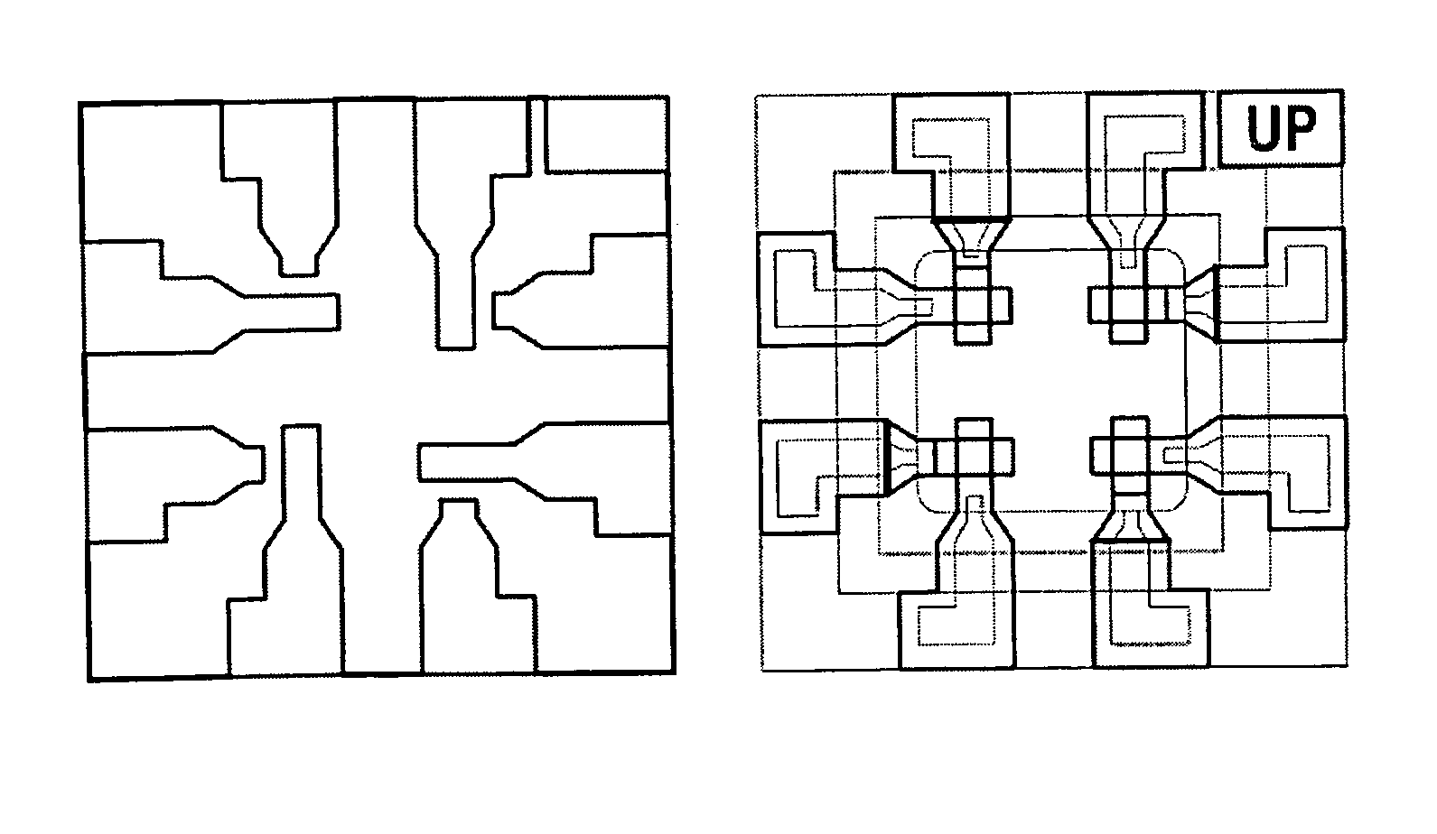
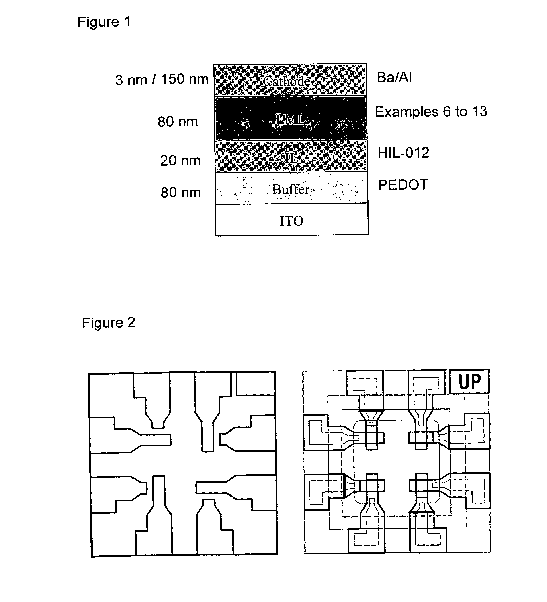
[0139]The OLED inks was ink jet printed using a Dimatix DMP 2800 printer on glass substrates (30 mm wide) covered with a 4 pixels structure of ITO, a PEDOT layer and HIL-012 layer. 6 mm squares were printed using 15, 20, 35 and 40 drop spacing (ds). Two drying procedures were used, a hot plate at 100° C. and vacuum at room temperature to assess the differences in film quality.

[0140]The HIL-012 layer did not wet or the swaths merge when using 35 and 40 ds. The printing performed better using 15 and 20 ds with better wetting but drying fronts seen on the film.

example 1

[0141]Essentially, Comparative Example 1 was repeated. However, an inert polymeric binder has been added to the printing ink. The printing ink comprised 0.4% by weight polystyrene having a weight average molecular weight of 200,000 g / mol (as supplied by Sigma Aldrich) and 1.6% by weight of the semiconducting compounds as mentioned in Comparative Example 1.

[0142]The HIL-012 layer was wetted acceptable for 25-40 ds and not all the swaths merge after printing. However, the results are improved in comparison to the Comparative example.

example 2

[0143]Essentially, Comparative Example 1 was repeated. However, an inert polymeric binder and a wetting agent have been added to the printing ink. The printing ink comprised 0.4% by weight polystyrene having a weight average molecular weight of 200,000 g / mol (as supplied by Sigma Aldrich), 1% by weight 3-ethoxy-1,1,1,2,3,4,4,5,5,6,6,6-dodecafluoro-2-trifluoromethyl-hexane (HFE 7500 commercially available from 3M™ NOVEC™ Engineered Fluid) and 1.6% by weight of the semiconducting compounds as mentioned in Comparative Example 1.

[0144]A good wetting of the HIL-012 layer was achieved. Nevertheless, small pinholes are visible on the layers for 20 ds and above. However, the results are improved in comparison to the Example 1.


PUM

PropertyMeasurementUnit
surface tensionaaaaaaaaaa
glass transition temperatureaaaaaaaaaa
boiling pointaaaaaaaaaa

Abstract

The present invention relates to novel compositions comprising light emitting materials and/or charge transport materials and a polymeric binder, to their use as conducting inks for the preparation of organic light emitting diode (OLED) devices, to methods for preparing OLED devices using the novel formulations, and to OLED devices prepared from such methods and formulations.

Description

RELATED APPLICATIONS[0001]This application is a national stage application (under 35 U.S.C. §371) of PCT / EP2010 / 007132, filed Nov. 24, 2010, which claims benefit of European Patent Application No. 09015911.2, filed Dec. 23, 2009.FIELD OF THE INVENTION[0002]The present invention relates to novel compositions comprising light emitting materials and / or charge transport materials and a polymeric binder, to their use as inks for the preparation of organic light emitting diode (OLED) devices, to methods for preparing OLED devices using the novel compositions, and to OLED devices prepared from such methods and compositions.BACKGROUND AND PRIOR ART[0003]When preparing OLED devices usually printing techniques like inkjet printing, roll to roll printing, slot dye coating or gravure printing are used to apply the active layer. Based on low solubility of the most of the present organic compounds useful as emitting materials and / or charge transport materials, these techniques need the use of sol...

Claims


Application Information

Patent Timeline
Patent Type & Authority Applications(United States)
IPC IPC(8): C09K11/06H01B1/12C09D7/63
CPCC08K5/0041Y02E10/549C08K5/56C09D5/24C09D7/1233C09D11/03C09D11/52H01L51/0005H01L51/0007H01L51/5016H05B33/20C09B57/00C09B57/008C09B57/10C09B1/00C08K5/0091C09D7/63C08G59/50C08G59/56C08L63/00Y02P70/50H10K71/15H10K71/135H10K50/11H10K2101/10
Inventor JAMES, MARKGONCALVES-MISKIEWICZ, MAGDAMAY, PHILIP EDWARDNANSON, LANAEFFENBERGER, RUTHBONRAD, KLAUSPAN, JUNYOUKLUGE, EDGAR
Owner MERCK PATENT GMBH
Why Eureka
Try Eureka