CVD diamond-coated composite substrate containing a carbide-forming material and ceramic phases and method for making same

a carbide-forming material and composite substrate technology, applied in the field of material products, can solve the problems of increasing the total manufacturing cost of semiconductor wafers, the total cost of polishing pads, the downtime of polishing pads to be replaced, and the cost of test wafers to recalibrate pads for a single wafer polishing run, etc., to overcome the shortcomings of conventional materials, strong and tough composite materials, and high adhesion of cvd diamond materials

Inactive Publication Date: 2005-12-15
BEST ENGINEERED SURFACE TECH LLC
View PDF57 Cites 70 Cited by
  • Summary
  • Abstract
  • Description
  • Claims
  • Application Information

AI Technical Summary

Benefits of technology

[0022] The present invention overcomes these prior art problems in the fabrication of CMP pad conditioners, cutting tool inserts and tips, wear components and heat spreaders via the use of a composite ceramic substrate for the deposition of CVD diamond. The present invention overcomes shortcomings in conventional materials by providing a CVD diamond coated ceramic material composite product that has the advantages of high adhesion of the CVD diamond material, and is a strong and tough composite material that is resistant to fracture at a low cost compared to conventional CVD diamond component products.
[0029] As used herein, the term “ceramic” is to be interpreted in its widest sense as including not only oxides but also non-oxide materials, for example such as, silicon carbide or silicon nitride. The ceramic material phases of the composite substrate of the present invention provide the stiffness required to maintain the diamond-coated composite product flat; the presence of the second phase material (the carbide-forming material) provides strength and toughness, resulting in a very strong, tough, and adherent composite diamond-coated product. As used herein, the term “carbide-forming material” means a material that is capable, under appropriate conditions, of formation of a covalently bonded compound with carbon in a carbide. It is believed that regions of the carbide-forming material react with the depositing CVD diamond material to form regions of bonded carbide structures at the interface between the substrate and the CVD diamond layer, resulting in strong adhesion of the diamond layer to the substrate.
[0030] In a more particular embodiment, the ceramic phase is composed of silicon carbide and the unreacted phase of carbide-forming material is silicon metal. This material, known as Reaction-Bonded Silicon Carbide (“RBSiC”), has considerably better fracture toughness than does pure silicon, and provides much better dimensional stability, resulting in a flatter CVD diamond-coated composite product, such as a polishing pad conditioner. In particular, reaction-bonded silicon carbide or graphite-silicon carbide composites having dispersed therein a dispersed phase of silicon metal, or having grains of silicon carbide dispersed within a silicon metal matrix, have been found to be particularly suitable substrates for CVD diamond coatings.
[0032] In addition, the invention relates to the discovery that damage to fixed abrasive pads (and other sensitive CMP pads) resulting from contact with conditioning heads can be considerably reduced by avoiding the presence of large diamond crystals in the conditioning head surface. Large crystals have been found to provide a disproportionate share of conditioning, but also to cause a disproportionate share of damage to the CMP polishing pad. A reduced level of such crystals was found to be obtainable through the preparation of conditioning heads surfaces that are significantly more homogeneous than previously available on previously described surfaces. However, this reduced number of large crystals and improved homogeneity of the surface results in the necessity to increase the down force applied to the conditioner in order to obtain the desired level of conditioning using commercially available CMP polishing equipment Increased homogeneity can be achieved by carefully controlling the particle size distribution of any diamond grit applied to the surface, carefully controlling the density of grit particles per unit area of the coated substrate, or growing a CVD diamond layer on pre-roughened substrates, so that the roughness of the diamond layer is in part determined by the surface roughness of the substrate.
[0056] In another embodiment, the invention relates to polishing pad conditioning heads having a substrate, and a CVD diamond coating deposited thereon, wherein the surface of the coating has an average roughness (Ra) of at least about 0.30 microns, more particularly, at least about 0.40 microns. It is believed that this degree of surface roughness can provide enhanced conditioning results on non-fixed abrasive pads, as compared to conditioning heads with lower roughness levels.
[0057] The conditioning head of the invention is suitable for the conditioning of polishing pads that require very gentle conditioning. The conditioning head for a CMP and similar types of apparatus has been found to condition the pads without unnecessary damage to the structure of the pad. This in turn has extended the life of the polishing pad without sacrificing wafer removal rates and methods for making the polishing pads. In addition, the conditioning head of the present invention:

Problems solved by technology

CMP represents a major portion of the production cost for semiconductor wafers.
The total cost for the polishing pad, the downtime to replace the pad and the cost of the test wafers to recalibrate the pad for a single wafer polishing run can be quite high.
In many complex integrated circuit devices, up to five CMP runs are required for each finished wafer, which further increase the total manufacturing costs for such wafers.
With polishing pads designed for use with abrasive slurries, the greatest amount of wear on the polishing pads is the result of polishing pad conditioning that is necessary to place the pad into a suitable condition for these wafer planarization and polishing operations.
However, such over-texturing of the pad results in a shortening of the pad life.
On the other hand, under-texturing results in insufficient material removal rate during the CMP step and lack of wafer uniformity.
While the weave of these pads is quite dense, there is opportunity for slurry particles to become trapped within the weave.
Efficiency of removal of used slurry components must be balanced against damage to the fibers of the weave caused by contact with the conditioning head surface, which can cause excessive breakage of the fibers.
These pads also require conditioning, because the CMP polishing rate obtained when using the pads is highly sensitive to the surface properties of the abrasive.
Initial “breaking in” periods for these polishing pads, during which consistent quality polishing is difficult to obtain, tend to be long, and the resulting loss of wafers is an added expense.
The use of such conventional conditioning heads is limited to the conditioning of polishing pads that have been used during oxide CMP wafer processing, i.e. when the exposed outer layer of the polishing pad is an oxide-containing material as opposed to metal.
However, the conditioning heads described above are ineffective for conditioning polishing pads used m metal CMP processing, because the slurry used to remove metal from the wafer can react with the nickel and degrade and otherwise dissolve the nickel outer layer of the conditioning head.
Dissolution of the nickel overcoat can result in a major loss of the diamond grit from the plate, potentially scratching the wafers.
In addition, these typical conditioning heads use relatively large sized diamond grit particles.
Rpm is the most meaningful measure of roughness for gritless CMP pads, since it provides an average of the peaks that are doing the bulk of the work during conditioning However, a new generation CMP pads, including fixed abrasive pads and many woven pads, cannot be conditioned by conventional conditioners because conditioning heads having grit particles larger than 15 microns are too rough; the large grit particles tend to damage the pad.
However, difficulties with this approach are the lack of independent control of the particle size and density of working diamond grains, and the resulting bow of the diamond-coated silicon substrate product.
While silicon has been used successfully as a substrate for CVD diamond in preparation of some CMP pad conditioners, in accordance with the invention of this application, it has been found that a silicon substrate does not provide sufficient rigidity to support diamond coatings of sufficient thickness to provide optimal CMP conditioning in some applications with sensitive pad materials.
Because of both internal growth stress in CVD diamond materials, and the mismatch in thermal coefficients of expansion between diamond and silicon, a CVD diamond-coated silicon substrate conditioning head will bow or bend, even when supported by a metal backing plate, resulting in a conditioner that is not completely flat.
A bowed conditioning head does not provide as consistent conditioning as a flat conditioning head, and is thus less desirable.
However, this material is not well suited as a substrate for growing CVD diamond because the deposition process reduces the hardness and strength of the steel.
Cemented tungsten carbide is also used frequently in making cutting tools, but CVD diamond does not adhere well to this material without either etching of the surface to remove cobalt, or application of an intermediate layer of material to increase adhesion.
Likewise, silicon nitride, another material used in the cutting tool industry, does not provide the high adhesion necessary for CVD diamond coatings for viable commercial application.
Use of molybdenum as a substrate results in a high CVD diamond nucleation density, but again the adhesion of CVD diamond to this substrate is poor.
CVD diamond does adhere well to silicon substrates, but silicon is too fragile and has a fracture toughness that is too low, to make it suitable as a substrate for cutting tools, wear parts or other mechanical applications.
In many applications, however, the use of freestanding CVD diamond substrates is inhibited either by the size of the die, the thickness of the die needed for retrofit into existing packages, and / or the cost of the diamond material for the given application.
The high shear forces and temperatures that are generated in, for example, a dry-running pump seal application, generally result in adhesion failure of CVD diamond coatings on typical pump seal materials, such as sintered silicon carbide.

Method used


Image

  • CVD diamond-coated composite substrate containing a carbide-forming material and ceramic phases and method for making same
  • CVD diamond-coated composite substrate containing a carbide-forming material and ceramic phases and method for making same
  • CVD diamond-coated composite substrate containing a carbide-forming material and ceramic phases and method for making same

Examples


example 1

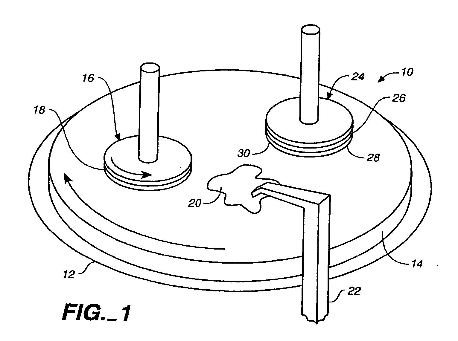
[0138] A two (2) inch diameter silicon substrate having a thickness of 0.04 inch (˜1 mm) was placed flat on a support fixture of an HFCVD reactor of the type described and claimed. in the above-referenced Garg, et al., U.S. Pat No. 5,186,973, as modified in the disclosure of U.S. Pat. Nos. 5,833,753 and 5,997,650, the entire contents of which are incorporated herein by reference. A monolayer of synthetic diamond grit having an average particle diameter of about 10 microns was uniformly distributed over the entire exposed surface of the first side of the silicon substrate to achieve an average grit density of 800 grains or grit particles per mm2 and a range from 700 to 900 grains per mm2. The grit from a container was uniformly distributed by using an air dispersion technique in which the grit was dropped at a controlled rate from a fixed height, above the wafer. A moving air current was used to disperse the grit in a lateral direction across the substrate.

[0139] The substrate was t...

example 2

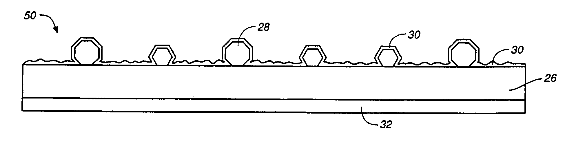
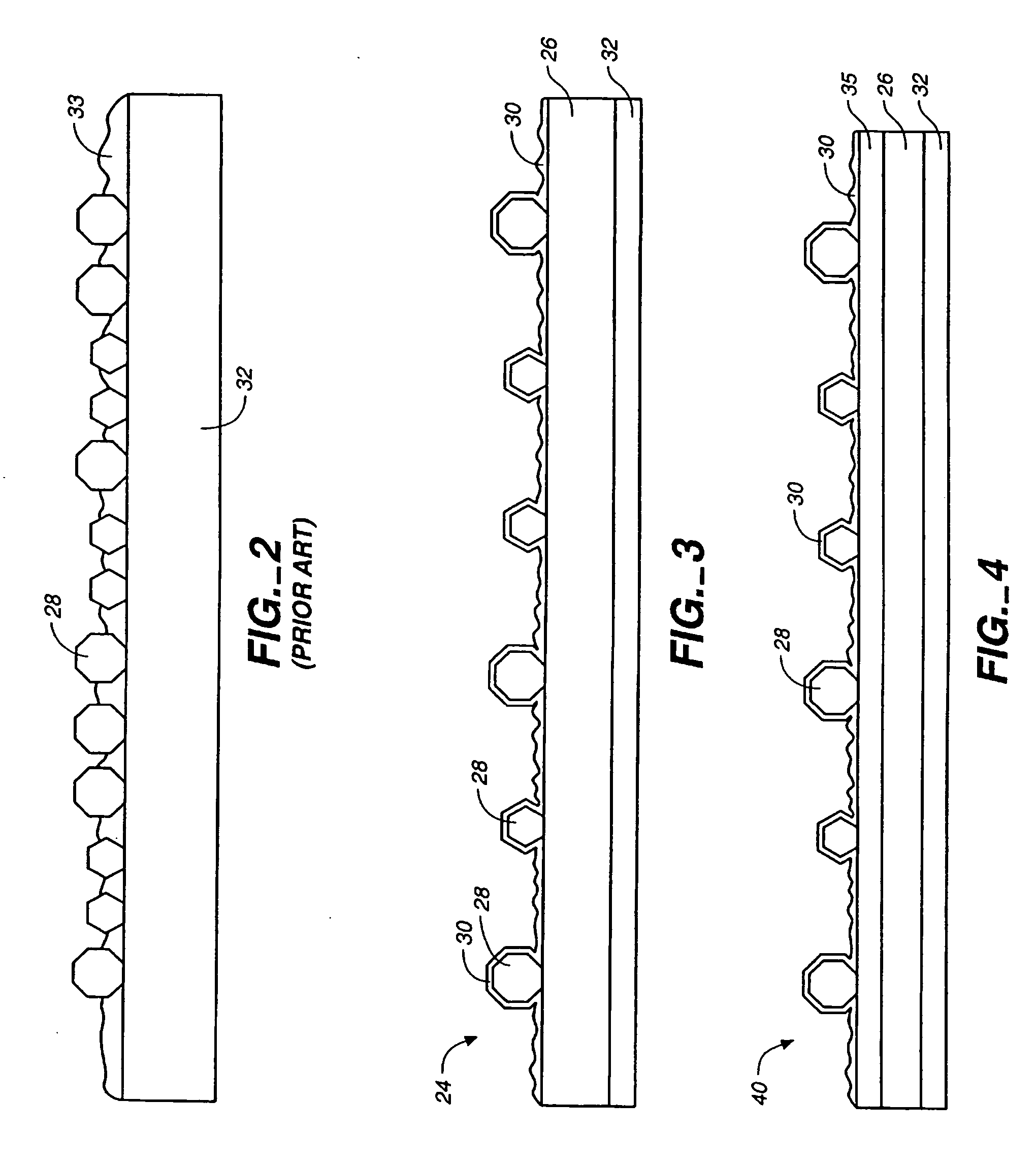
[0141] A 2″ diameter by 0.135″ thick round substrate of PUREBIDE R2000 reaction-bonded silicon carbide material which was surface-finished by through feed grinding was seeded with 1-2 micron diamond by mechanically rubbing the surface. The excess diamond was then removed from the surface. Diamond grit (10 micron size) was then dispersed on the surface of the substrate with a density of approximately 420 particles per mm2. The sample was then placed in CVD deposition reactor and a layer of CVD diamond about 8 microns thick was deposited on the surface by the process outlined in Example #1. The sample was then examined and found to have a uniform adherent diamond coating. The bow of the coated substrate was found to be approximately 5 + / −2 microns across the 2-inch diameter substrate. This value was, within measurement error, the same as the bow of the substrate prior to diamond coating. The 10 micron diamond crystals were strongly adhered to the surface. The sample was then hand rubb...

example 3

[0142] A 2″ diameter by 0.135″ thick round substrate of PUREBIDE R2000 material with a lapped surface finish was seeded with 1-2 micron diamond by mechanically rubbing the surface. The excess diamond was then removed from the surface. Diamond grit (75 micron size) was then dispersed on the surface of the substrate with a density of 10 particles per mm2. The sample was then placed in CVD deposition reactor and a CVD diamond layer about 15 microns thick was deposited on the surface by the process outlined in Example #1. The sample was then examined and found to have a uniform adherent diamond coating. The 75 micron diamond crystals were strongly adhered to the surface. The sample was then hand rubbed on a polyurethane CMP polishing pad and reexamined. No indications of grit pullout were found.


PUM

PropertyMeasurementUnit
average grain sizeaaaaaaaaaa
grain sizeaaaaaaaaaa
diameteraaaaaaaaaa

Abstract

The present invention relates to a composite material and the method of making same ,which comprises a CVD diamond coating applied to a composite substrate of ceramic material and an unreacted carbide-forming material of various configurations and for a variety of applications. One example of the composite material is a composite of SiC and free silicon metal known as Reaction-Bonded Silicon Carbide. Several examples of applications of the invention include: 1) heads or disks for conditioning polishing pads, including pads used in Cheniical-Mechanical-Planarization, 2) cutting and dressing tool inserts and tips, 3) heat spreaders for electronic devices, and 4) wear components including mechanical seals and pump seals.

Description

BACKGROUND OF THE INVENTION [0001] 1. Field of the Invention [0002] The present invention relates to a material product comprising a layer of CVD diamond coating applied to a composite substrate of ceramic material and a carbide-forming material of various configurations and for a variety of applications, and methods for manufacturing these products. The products of the invention have utility in a wide variety of applications, which include: heads or disks for the conditioning of polishing pads, including pads used in Chernical-Mechanical-Planarization (CMP), cutting and dressing tool inserts and tips, wear components, such as mechanical seals and pump seals, and heat spreaders for electronic devices. [0003] 2. Description of Related Art [0004] CMP is an important process in the fabrication of integrated circuits, disk drive heads, nano-fabricated components, and the like. For example, in patterning semiconductor wafers, advanced small dimension patterning techniques require an abso...

Claims


Application Information

Patent Timeline
Patent Type & Authority Applications(United States)
IPC IPC(8): B24B37/04B24B53/12B24D18/00C04B41/50C04B41/85C23C16/27F16J15/34
CPCB24B53/017Y10T428/30B24D18/0018C04B41/009C04B41/5002C04B41/85C23C16/271F16J15/3496B24B53/12C04B41/4531C04B35/565C04B35/573
Inventor SLUTZ, DAVID E.FINKE, STEVEN J.
Owner BEST ENGINEERED SURFACE TECH LLC
Why Eureka
Try Eureka