Programmable resistive device and memory using diode as selector

a resistive device and selector technology, applied in static storage, digital storage, instruments, etc., can solve the problems of reliability problems, large cell size of electrical fuse using silicided polysilicon, and high program voltage of fuse, so as to reduce cell size and cost

Active Publication Date: 2017-11-14
ATTOPSEMI TECH CO LTD
View PDF301 Cites 206 Cited by
  • Summary
  • Abstract
  • Description
  • Claims
  • Application Information

AI Technical Summary

Benefits of technology

[0012]Embodiments of Programmable Resistive Device (PRD) cells with coupling between PRDs built in the contact pillars of crossovers of multiple-layer conductor arrays are disclosed. The programmable resistive devices can be fabricated in standard CMOS logic compatible processes with minimum mask increments to reduce cell size and cost.
[0013]A Programmable Resistive Device (PRD) includes one Programmable Resistive Element (PRE) and one diode selector built in a contact / via pillar at a crossover of two conductor lines. In one embodiment, the Programmable Resistive Element (PRE) or diode of one 3D PRD can be coupled to a PRE or diode of another PRD in a single-diode PRD cell. In another embodiment, a PRE can be shared between two PRDs in a vertical or horizontal direction in a 3D PRD array to create a dual-diode PRD cell. The two diodes can conduct currents in the opposite directions for programming 0 and 1, respectively. The former can be applied to electrical fuse, PCRAM (Phase-Change RAM), or unipolar-switch RRAM (Resistive RAM). The latter can be applied to MRAM (Magnetic RAM) or bipolar-switch RRAM. A Programmable Resistive Device (PRD) can use a p-i-n or P / N diode as selector and a Programmable Resistive Element (PRE) built vertically inside a contact pillar. Contact pillars can be constructed in the crossovers of at least two conductor arrays in at least two vertical planes running in substantially perpendicularly directions. There can be more than two conductor layers to construct a plural of memory arrays on top of each other in a single integrated circuit. The programmable resistive element (PRE) can be an electrical fuse for One-Time Programmable (OTP) memory, or can be a phase-change material or resistance change film for building Phase Change RAM (PCRAM) or Resistive RAM (RRAM), respectively, or can be a Magnetic Tunnel Junction (MTJ) for building Magnetic RAM (MRAM). Because the cell size only depends on the pitches of two cross-over conductors (i.e. 4F2 cell where F stands for Figure size), and the conductors can be stacked vertically in multiple layers (i.e. k+1 layers), the effective cell size is 4F2 / k for single-diode PRD cells and 4F2 / (2 k) for dual-diode PRD cells, thus, costs can be reduced substantially for variously applications, such as embedded applications.

Problems solved by technology

As a result, the cell size of an electrical fuse using silicided polysilicon tends to be very large.
Moreover, the anti-fuse requires very high program voltage with large current to breakdown dielectrics, has wide post-program resistance distribution, and sometimes has reliability issues.
In the advanced CMOS technologies beyond 40 nm, the nanometer devices cannot sustain voltage higher than 4.0V, not to mention about requiring large areas to build high voltage devices and charge pumps.

Method used


Image

  • Programmable resistive device and memory using diode as selector
  • Programmable resistive device and memory using diode as selector
  • Programmable resistive device and memory using diode as selector

Examples


Embodiment Construction

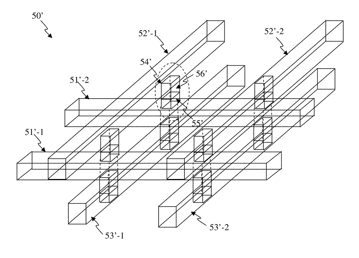
[0051]The present invention relates to programmable memory devices, such as programmable resistive devices for use in memory arrays, built in contact pillars at the cross-over of multiple-layer conductors.

[0052]Embodiments disclosed herein can use at least two arrays of conductor lines in at least two vertical layers to build a Programmable Resistive Device (PRD) in at least one cross-over of the conductor lines. The conductor lines can run in substantially perpendicular directions in alternative layers. A programmable resistive device can be built at the cross-over (i.e. contact) of two conductor lines in two vertical layers. A programmable resistive device has a programmable resistive element (PRE) coupled to one terminal of a diode built vertically and another end coupled to a first conductor. At least one PRE of one PRD can be coupled to a diode or PRE of another PRD in a single-diode PRD cell according to one embodiment. At least one PRE of two PRDs can be shared to create a du...


PUM


Abstract

Building programmable resistive devices in contact holes at the crossover of a plurality of conductor lines in more than two vertical layers is disclosed. There are plurality of first conductor lines and another plurality of second conductor lines that can be substantially perpendicular to each other, though in two different vertical layers. A diode and / or a programmable resistive element can be fabricated in the contact hole between the first and second conductor lines. The programmable resistive element can be coupled to another programmable resistive device or shared between two programmable devices whose diodes conducting currents in opposite directions and / or coupled to a common conductor line. The programmable resistive memory can be configured to be programmable by applying voltages to conduct current flowing through the programmable resistive element to change its resistance for a different logic state.

Description

CROSS-REFERENCE TO RELATED APPLICATIONS[0001]This application claims priority benefit of U.S. Provisional Patent Application No. 61 / 734,945, filed on Dec. 7, 2012 and entitled “CIRCUIT AND SYSTEM OF 3D PROGRAMMABLE RESISTIVE DEVICE AND MEMORY USING DIODE AS SELECTOR,” which is hereby incorporated herein by reference.[0002]This application also claims priority benefit of U.S. Provisional Patent Application No. 61 / 880,916, filed on Sep. 21, 2013 and entitled “CIRCUIT AND SYSTEM OF USING JUNCTION DIODE AS PROGRAM SELECTOR FOR ELECTRICAL FUSES WITH EXTENDED AREA FOR ONE-TIME PROGRAMMABLE DEVICES,” which is hereby incorporated herein by reference.BACKGROUND OF THE INVENTION[0003]A programmable resistive device is generally referred to a device with a resistance state that may change by means of programming. Resistance states can also be determined by resistance values. For example, a resistive device can be a One-Time Programmable (OTP) device, such as electrical fuse, and the programmin...

Claims


Application Information

Patent Timeline
Patent Type & Authority Patents(United States)
IPC IPC(8): G11C13/00G11C17/18G11C17/16
CPCG11C13/0069G11C13/004G11C13/0004G11C17/16G11C17/18G11C13/0007G11C2213/74G11C2213/72
Inventor CHUNG, SHINE C.
Owner ATTOPSEMI TECH CO LTD
Why Eureka
Try Eureka