Substrates for liquid crystal panels and liquid crystal panels

a technology of liquid crystal panels and substrates, applied in non-linear optics, instruments, optics, etc., can solve the problems of increasing the thickness of the liquid crystal display module, and achieve the effect of greatly enhancing the color reproduction reducing the thickness of the second substrate, and greatly reducing the thickness of the liquid crystal panel

Active Publication Date: 2018-01-02
WUHAN CHINA STAR OPTOELECTRONICS TECH CO LTD
View PDF1 Cites 5 Cited by
  • Summary
  • Abstract
  • Description
  • Claims
  • Application Information

AI Technical Summary

Benefits of technology

[0004]The present disclosure relates to a substrate for liquid crystal panels, and the liquid crystal panel incorporated with the substrate, wherein the substrate may operate as a color filterer, a polarizer, and a metal electrode. Not only the color saturation and the color reproduction may be enhanced, but also the thickness of the liquid crystal panel may be reduced.
[0015]In view of the above, the band-pass width of the wire grid layer of the second substrate may precisely match with the backlight peak such that the color reproduction of the liquid crystal panel may be greatly enhanced. At the same time, the second substrate 30 includes periodically arranged metal layer and the dielectric layer of the sandwich structure. Thus, the second substrate may operate as the color filter, the polarizer, and the metal electrode. Compared to the conventional configuration of the color filter, the polarizer, and the metal electrode, the proposed solution may greatly reduce the thickness of the second substrate such that the thickness of the liquid crystal panel may be greatly reduced.

Problems solved by technology

As shown in FIG. 1, the thickness of the combined top polarizer and the color filter is large, which results in an increasing thickness of the liquid crystal display module.

Method used


Image

  • Substrates for liquid crystal panels and liquid crystal panels
  • Substrates for liquid crystal panels and liquid crystal panels
  • Substrates for liquid crystal panels and liquid crystal panels

Examples


Embodiment Construction

[0024]Embodiments of the invention will now be described more fully hereinafter with reference to the accompanying drawings, in which embodiments of the invention are shown.

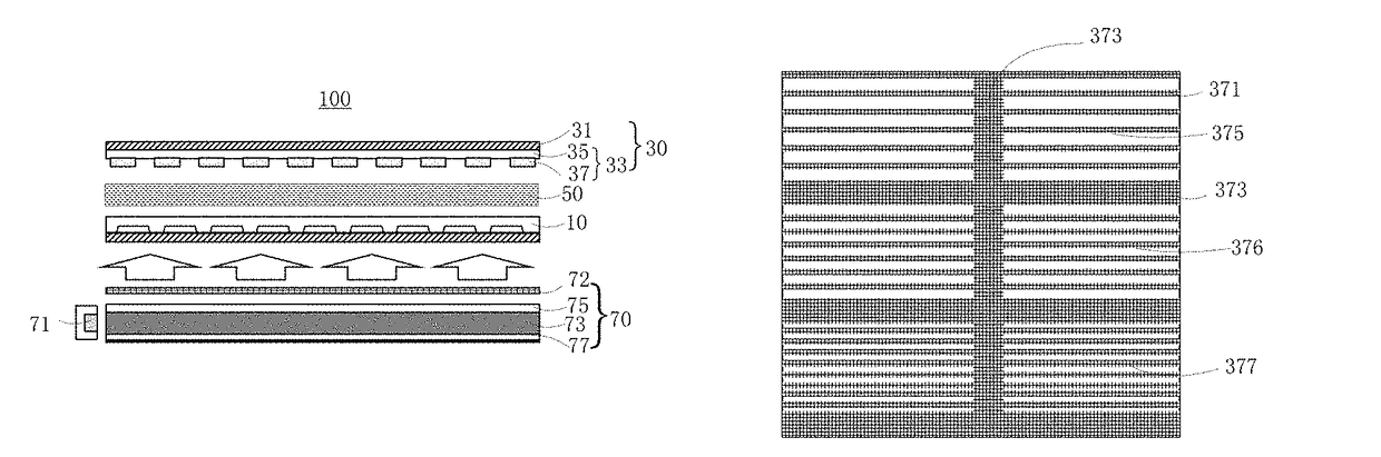
[0025]FIG. 2 is a cross-sectional view of the liquid crystal panel in accordance with one embodiment. The liquid crystal panel 100 includes a first substrate 10, a second substrate 30, a liquid crystal layer 50, and a backlight module 70. The first substrate 10 is opposite to the second substrate 30. The liquid crystal layer 50 is arranged between the first substrate 10 and the second substrate 30. The backlight module 70 is arranged below the first substrate 10, that is, the backlight module 70 is arranged on a surface of the first substrate 10 facing away the second substrate 30.

[0026]The first substrate 10 is an array substrate. It can be understood that the pixel arrangement of the first substrate 10 may be of single-domain or multi-domains.

[0027]The second substrate 30 includes a glass substrate 31 and a wir...


PUM

PropertyMeasurementUnit
heightaaaaaaaaaa
heightaaaaaaaaaa
band-pass widthaaaaaaaaaa

Abstract

A substrate of liquid crystal panels includes a glass substrate, and a wire grid layer including a dielectric layer arranged on one side of the glass substrate, and a metal layer on the dielectric layer. The metal layer includes a number of first metal bars and a number of second metal bars. The second metal bars are configured to divide the metal layer into a first area, a second area, and a third area cyclically arranged. The first metal bars are arranged within the first area, the second area, and the third area in sequence, and the first metal bars are parallel to and are spaced apart from each other. The first metal bars within the different areas respectively include a first period, a second period, and a third period different from each other. In addition, the present disclosure also relates to a liquid crystal panel.

Description

BACKGROUND OF THE INVENTION1. Field of the Invention[0001]The present disclosure relates to liquid crystal display technology, and more particularly to a substrate for liquid crystal panels, and a liquid crystal panel.2. Discussion of the Related Art[0002]High gamut display panels are capable of displaying more colors, and are characterized by high color saturation and color reproduction. Thus, the high gamut display panels are favored by consumers.[0003]Currently, display panel manufactures continuously enhance the color gamut in response to the color reproduction demand from consumers. The proposed solutions include adjusting the location of the backlight peak, adopting RG fluorescent powder, adopting quantum dot (QD) backlight technology, and adjusting the location of the band-pass and the width of the half-peak of the color filters. Along with the standard named as REC.2020, the QD backlight technology has been developed. For instance, the companies, such as 3M, nanosys, and QD ...

Claims


Application Information

Patent Timeline
Patent Type & Authority Patents(United States)
IPC IPC(8): G02F1/1335G02F1/1343
CPCG02F1/133528G02F1/134336G02F2001/134345G02F2203/34G02F2001/133548G02F1/1333G02F1/133302G02F1/133548G02F1/134309G02F1/134345
Inventor ZHA, GUOWEI
Owner WUHAN CHINA STAR OPTOELECTRONICS TECH CO LTD
Why Eureka
Try Eureka