Circuit device, electro-optical device, and electronic apparatus

a technology of electrooptical devices and circuit devices, applied in static indicating devices, cathode-ray tube indicators, instruments, etc., can solve the problems of large current flow, inability to restore the boost operation of the boost circuit to a normal state, and the inability to turn off the supply to the display driver

Active Publication Date: 2018-01-02
SEIKO EPSON CORP
View PDF9 Cites 0 Cited by
  • Summary
  • Abstract
  • Description
  • Claims
  • Application Information

AI Technical Summary

Benefits of technology

[0007]According to some aspects of the invention, it is possible to provide a circuit device that is capable of detecting an abnormality of a boosted voltage generated by a boost circuit and allowing a boost operation of the boost circuit to recover to a normal state, as well as an electro-optical device, an electronic apparatus, and the like.
[0009]According to this aspect of the invention, the abnormality detection circuit detects an abnormality of the i-th boosted voltage, thereby enabling self-detection of an abnormality of a boosted voltage by the circuit device. If an abnormality of the i-th boosted voltage is detected, the j-th boost circuit that is different from the i-th boost circuit performs the low-capacity boost operation or stops the boost operation. Thus, the i-th boosted voltage can recover to a normal voltage, and the boost operation of the boost circuit can recover to a normal state.
[0018]If an abnormality of the i-th boosted voltage is detected, the j-th boost circuit performs the low-capacity boost operation and can thus generate the j-th boosted voltage. In the case where the i-th boosted voltage is generated based on the j-th boosted voltage, the generation of the j-th boosted voltage allows generation of the i-th boosted voltage, and therefore self-recovery from the power supply abnormality is possible.
[0030]A detection voltage having hysteresis characteristics can suppress repetition of an inversion of normality and abnormality with respect to the abnormality detection result when the i-th boosted voltage is near the detection voltage.
[0032]Providing the detection transistor TDET between the node for the first power supply voltage, which is not a boosted voltage, and the node for the i-th boosted voltage and inputting the input voltage VNB1 based on the second power supply voltage, which is not a boosted voltage, to the gate of the detection transistor TDET makes it possible to accurately detect an abnormality of the i-th boosted voltage when a boosted voltage abnormality occurs.

Problems solved by technology

In a display driver in which a power supply for driving is generated by the boost operations as described above, noise, data corruption of register values, and the like cause a large current to flow through a parasitic bipolar or the like of a boost circuit.
Thus, malfunction of the power supply occurs, making it impossible for the boost operation of the boost circuit to recover to a normal state.
However, with regard to display drivers for automobile applications, the power supplied to a display driver cannot be turned off unless an engine is shut off, for example, and thus recovery from malfunction of the power supply is difficult.
For example, if the substrate is a P-type substrate, the substrate voltage is the lowest voltage, and thus when a power supply abnormality occurs, the current flowing through a parasitic bipolar is highly likely to finally flow into the substrate.

Method used


Image

  • Circuit device, electro-optical device, and electronic apparatus
  • Circuit device, electro-optical device, and electronic apparatus
  • Circuit device, electro-optical device, and electronic apparatus

Examples


Embodiment Construction

[0052]The following describes preferred embodiments of the invention in detail. It should be noted that the embodiments to be described hereinafter are not intended to unduly limit the subject matter of the invention as set forth in the claims and that not all of the configurations to be described in the embodiments are necessarily essential as the means for achieving the invention. For example, although a case in which a circuit device is a driver is taken as an example in the following description, the invention is applicable to any circuit device that includes a power supply circuit having a boost circuit.

[0053]1. First Configuration Example

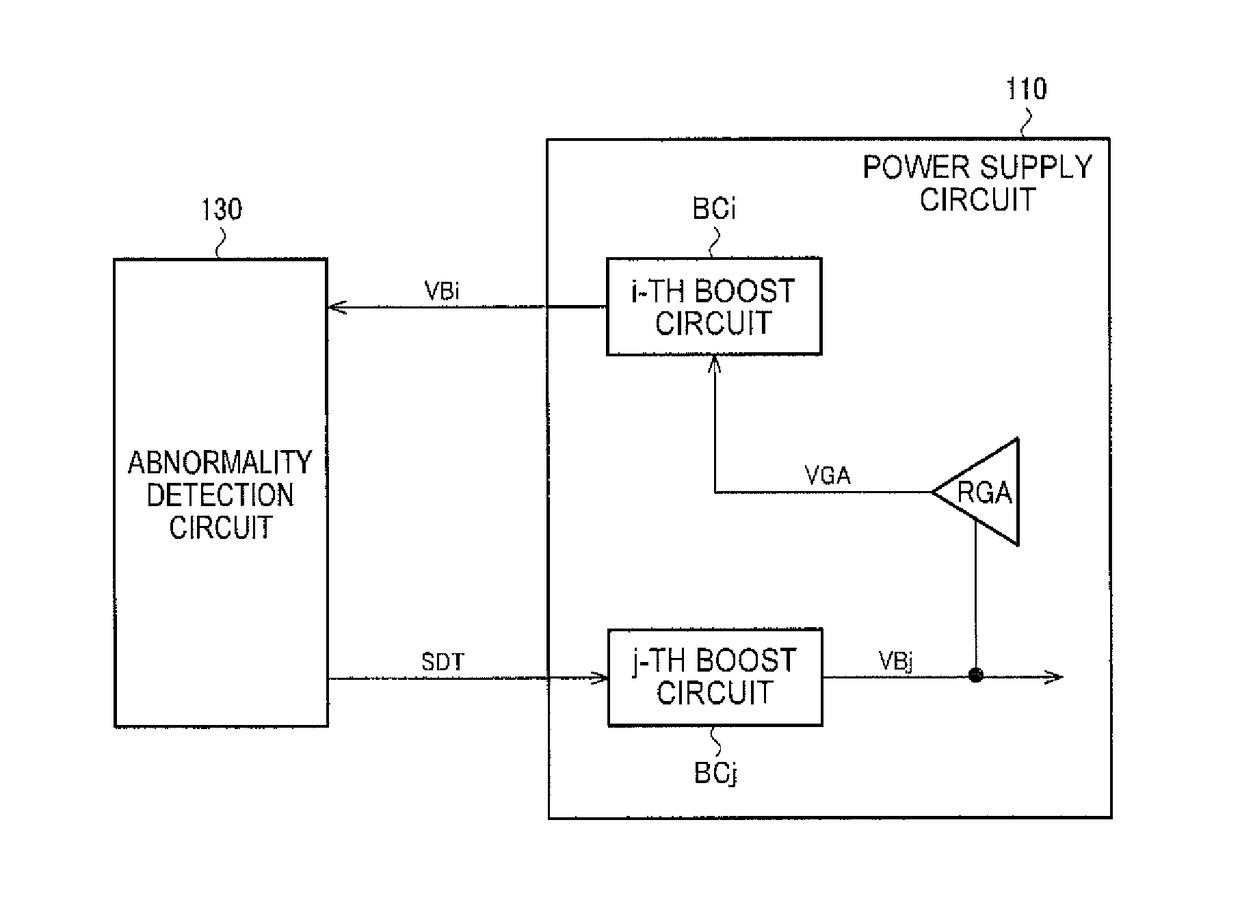
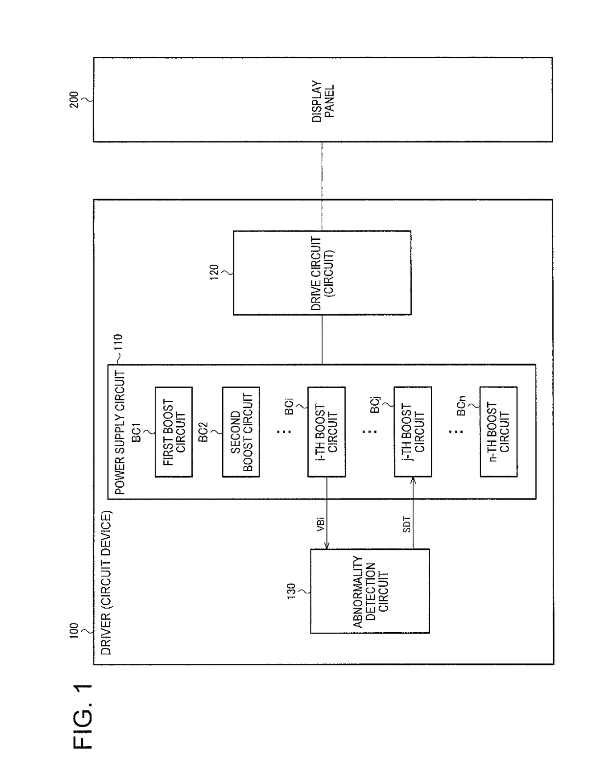
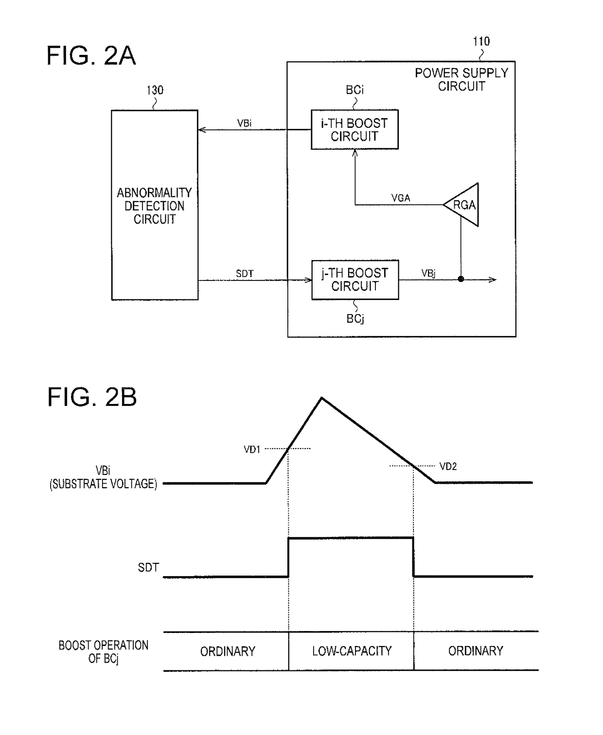
[0054]As described above, a driver that drives a display panel generates a plurality of voltages using a power supply circuit and causes circuits such as a source driver to operate with the plurality of voltages. As will be described later with reference to FIGS. 10 and 11, for example, a power supply circuit 110 of a driver 100 generates powe...


PUM


Abstract

A driver includes a power supply circuit having first to n-th boost circuits, a circuit that operates based on power supplied from the power supply circuit, and an abnormality detection circuit. The abnormality detection circuit detects an abnormality of an i-th boosted voltage that is generated based on a boost operation of an i-th boost circuit. If an abnormality of the i-th boosted voltage is detected, a j-th boost circuit performs a low-capacity boost operation with a lower current-supply capacity than an ordinary boost operation or stops the boost operation.

Description

BACKGROUND[0001]1. Technical Field[0002]The present invention relates to a circuit device, an electro-optical device, an electronic apparatus, and the like.[0003]2. Related Art[0004]Display drivers that drive display panels require various kinds of voltages such as, for example, a power supply for a source driving amplifier, a power supply for a gate driving amplifier, a power supply for a gradation voltage generation circuit, a common voltage for a display panel, and the like, and thus incorporate power supply circuits that generate the required voltages. For example, JP-A-2007-212897 and JP-A-2010-145738 disclose a display driver including a power supply circuit having a plurality of boost circuits (primary to quaternary boost circuits) as well as a source driver and a gate driver that are operated with power supplies generated by boost operations of the boost circuits of the power supply circuit.[0005]In a display driver in which a power supply for driving is generated by the boo...

Claims


Application Information

Patent Timeline
Patent Type & Authority Patents(United States)
IPC IPC(8): G09G1/00G09G3/00
CPCG09G3/006G09G2330/021G09G2330/12G09G2330/04G09G2330/028
Inventor NISHIMURA, MOTOAKI
Owner SEIKO EPSON CORP
Why Eureka
Try Eureka