Imaging device, operating method thereof, and electronic device

a technology of an electronic device and an imager, which is applied in the direction of radio frequency controlled devices, transistors, television systems, etc., can solve the problems of narrow dynamic range, detection range of illumination, etc., and achieve the effect of reducing the area of one pixel, high resolution and reducing the area of pixel

Inactive Publication Date: 2018-02-06
SEMICON ENERGY LAB CO LTD
View PDF17 Cites 6 Cited by
  • Summary
  • Abstract
  • Description
  • Claims
  • Application Information

AI Technical Summary

Benefits of technology

[0014]To make an image sensor have high resolution, the area of one pixel needs to be reduced. When the pixel area is reduced, the light-receiving area of a photoelectric conversion element is also reduced; as a result, the photosensitivity is lowered. In particular, in imaging under a low illuminance condition, the S / N ratio of imaging data largely decreases in some cases. That is, in the image sensor having the conventional structure, there is a trade-off between resolution and photosensitivity.
[0016]Thus, one object of one embodiment of the present invention is to provide an imaging device or the like having a novel structure in which a wide dynamic range can be achieved in imaging using a photoelectric conversion element utilizing an avalanche multiplication phenomenon. Another object of one embodiment of the present invention is to provide an imaging device or the like having a novel structure with high photosensitivity.
[0017]Alternatively, an object of one embodiment of the present invention is to provide an operating method or the like of an imaging device having a novel structure capable of broadening a dynamic range in imaging using a photoelectric conversion element utilizing an avalanche multiplication phenomenon. Another object of one embodiment of the present invention is to provide an operating method or the like of an imaging device having a novel structure with high photosensitivity.
[0030]One embodiment of the present invention can provide an imaging device or the like having a novel structure in which a wide dynamic range can be achieved in imaging using a photoelectric conversion element utilizing an avalanche multiplication phenomenon. In addition, one embodiment of the present invention can provide an imaging device or the like having a novel structure with high photosensitivity.
[0031]In addition, one embodiment of the present invention can provide an operating method or the like of an imaging device having a novel structure in which a wide dynamic range can be achieved in imaging using a photoelectric conversion element utilizing an avalanche multiplication phenomenon. In addition, one embodiment of the present invention can provide an operating method or the like of an imaging device having a novel structure with high photosensitivity.
[0032]In addition, one embodiment of the present invention can provide a novel imaging device, an operating method of the novel imaging device, a novel electronic device, or the like.

Problems solved by technology

However, the flowing current is larger in imaging which uses the photoelectric conversion element utilizing an avalanche multiplication phenomenon than in imaging which does not utilize the avalanche multiplication phenomenon; thus, due to the limit of the amount of accumulated charge in imaging, the detection range of illuminance, i.e., the dynamic range is narrowed.

Method used


Image

  • Imaging device, operating method thereof, and electronic device
  • Imaging device, operating method thereof, and electronic device
  • Imaging device, operating method thereof, and electronic device

Examples


embodiment 1

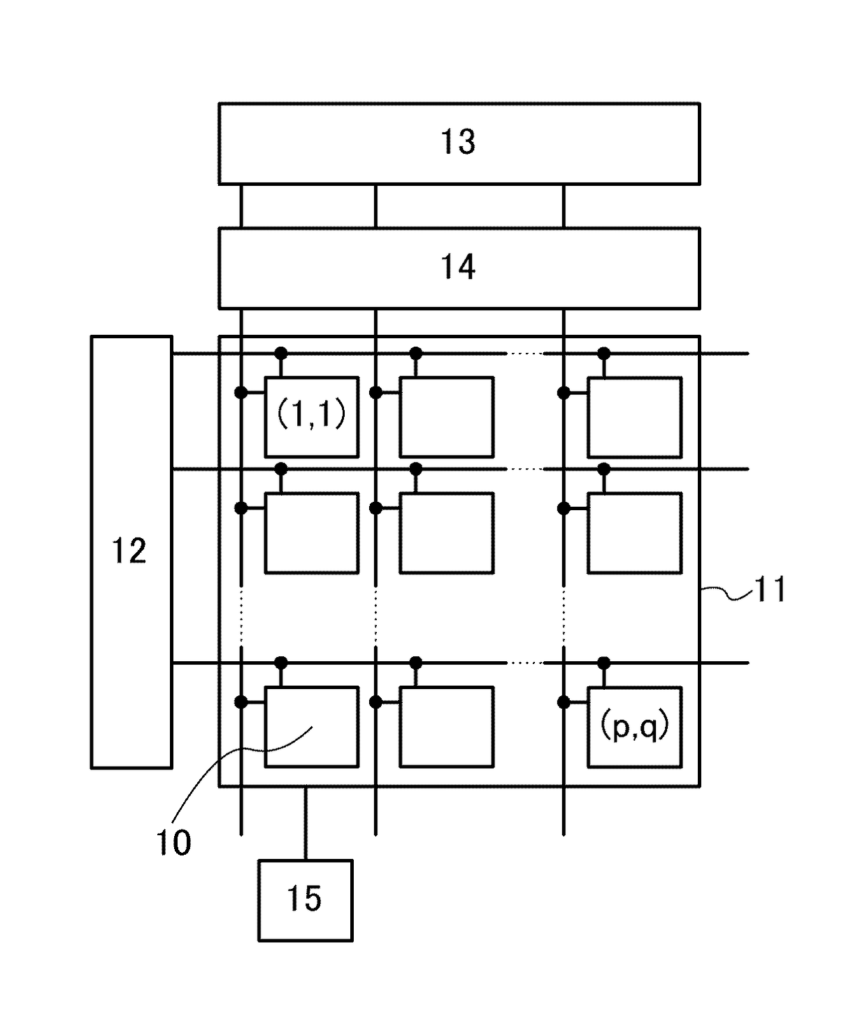
[0108]An imaging device of one embodiment of the present invention is described with reference to drawings.

[0109]In this specification and the like, an imaging device refers to any device that has an imaging function. The imaging device also indicates a circuit having a function of imaging or an entire system including such a circuit.

[0110]One embodiment of the present invention is an imaging device which has a function of suppressing a writing current flowing to a pixel including a photoelectric conversion element when an avalanche multiplication phenomenon occurs in the photoelectric conversion element, for example. Thus, for example, even when the avalanche multiplication phenomenon occurs to obtain the imaging data, the dynamic range can be broadened. That is, both the high photosensitivity and the wide dynamic range can be achieved.

[0111]FIG. 1 is a block diagram illustrating the configuration of an imaging device of one embodiment of the present invention. The imaging device i...

embodiment 2

[0204]In this embodiment, modification examples of the pixel 10 of the imaging device of one embodiment of the present invention are described with reference to drawings.

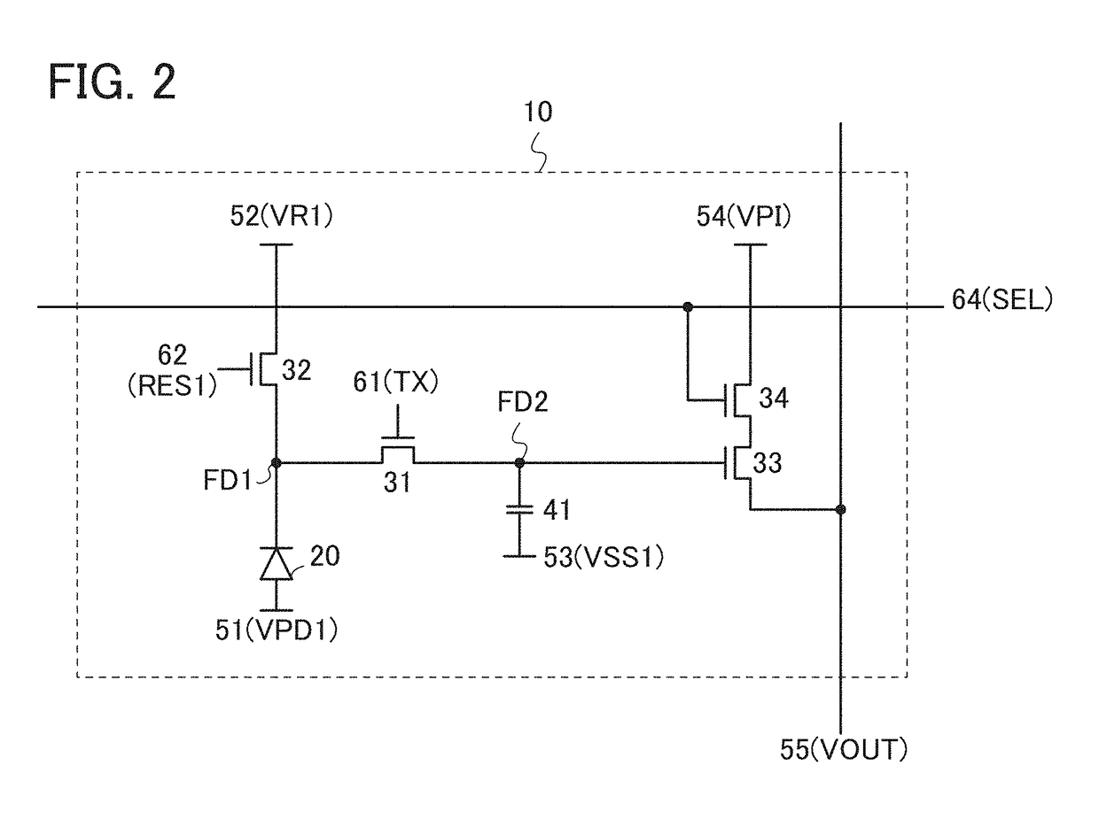
[0205]The pixel 10 included in the imaging device of one embodiment of the present invention can have a configuration illustrated in FIG. 15A as well as the configuration illustrated in FIG. 2. FIG. 15A is different from FIG. 2 in that the transistors 31 to 34 are all p-ch transistors. When the magnitude relationships of the potentials are reversed as appropriate, for example, FIG. 3 and FIG. 4A can be referred to for the operations in the normal imaging mode and in the wide dynamic range mode, respectively. Note that some of the transistors 31 to 34 may be p-ch transistors. Alternatively, CMOS transistors may be employed.

[0206]Although the transistor 34 lies between the transistor 33 and the wiring 54 (VPI) in FIG. 2, the transistor 33 may lie between the transistor 34 and the wiring 54 (VPI) as shown in FIG. 15B.

[...

embodiment 3

[0245]In this embodiment, specific structure examples of the imaging device of one embodiment of the present invention will be described below with reference to drawings.

[0246]FIG. 20A illustrates an example of a cross-sectional view of the imaging device of one embodiment of the present invention and illustrates a specific connection between the photoelectric conversion element 20, the transistor 31, and the transistor 32 which are included in each of the pixels 10 in FIG. 1. Note that the transistors 33 and 34 are not illustrated in FIG. 20A. The imaging device includes a tier 1100 including the transistors 31 to 34 and a tier 1200 including the photoelectric conversion element 20.

[0247]Although the wirings, electrodes, and conductors 91 are illustrated as independent components in cross-sectional views in this embodiment, some of them are provided as one component in some cases when they are electrically connected to each other. In addition, a structure in which a gate, a source,...


PUM


Abstract

An imaging device whose dynamic range is broadened is provided. The imaging device includes a pixel including a first photoelectric conversion element and a first circuit including a second photoelectric conversion element. The first circuit switches the operation mode of the pixel to a normal imaging mode or a wide dynamic range mode and switches the operation region of the first photoelectric conversion element to a normal region or an avalanche region in accordance with the illuminance of light with which the second photoelectric conversion element is irradiated. When the illuminance of light with which the first photoelectric conversion element is irradiated is increased, the increase rate of a writing current flowing to the pixel is higher in the avalanche region than in the normal region. However, in the wide dynamic range mode, the increase rate of current can be lowered, and thus the dynamic range can be broadened.

Description

BACKGROUND OF THE INVENTION[0001]1. Field of the Invention[0002]One embodiment of the present invention relates to an imaging device and an electronic device.[0003]Note that one embodiment of the present invention is not limited to the above technical field. The technical field of the invention disclosed in this specification and the like relates to an object, a method, or a manufacturing method. In addition, one embodiment of the present invention relates to a process, a machine, manufacture, or a composition of matter. Specifically, examples of the technical field of one embodiment of the present invention disclosed in this specification include a semiconductor device, a display device, a light-emitting device, a power storage device, an imaging device, a memory device, a method for driving any of them, and a method for manufacturing any of them.[0004]2. Description of the Related Art[0005]A technique by which transistors are formed using oxide semiconductor thin films formed over...

Claims


Application Information

Patent Timeline
Patent Type & Authority Patents(United States)
IPC IPC(8): H01L27/146H04N5/3745H04N5/232H04N5/374H04N5/353H04N5/369H04N5/355
CPCH01L27/14612H01L27/14607H01L27/14616H01L27/14636H01L27/14645H01L27/14663H01L27/14665H01L27/14689H04N5/23245H04N5/355H04N5/3532H04N5/3559H04N5/3698H04N5/374H04N5/3745H01L2924/15311H01L2224/48091H01L2224/48227H01L2924/00014H04N23/667H04N25/531H04N25/57H04N25/59H04N25/709H04N25/77H04N25/76
Inventor OHMARU, TAKURO
Owner SEMICON ENERGY LAB CO LTD
Why Eureka
Try Eureka