Supercharge Your Innovation With Domain-Expert AI Agents!

Positioning method in microprocessing process of bulk silicon

a microprocessing and bulk silicon technology, applied in the field of semiconductors, can solve problems such as poor alignment accuracy, and achieve the effect of greatly improving the alignment accuracy of the microprocessing process for bulk silicon

Active Publication Date: 2018-02-27
CSMC TECH FAB2 CO LTD
View PDF15 Cites 0 Cited by
  • Summary
  • Abstract
  • Description
  • Claims
  • Application Information

AI Technical Summary

Benefits of technology

[0003]Accordingly, it is necessary to provide positioning method in micromachining process for a bulk silicon which can effectively enhance an alignment accuracy.
[0005]In aforementioned positioning method in micromachining process for a bulk silicon, a method combining the double-sided lithography to the stepper lithography is adopted, the stepper lithography machine alignment mark for the stepper lithography machine on the first substrate is found by the double-sided lithography machine, and then the second substrate is directly aligned by the stepper lithography machine. The alignment accuracy of the stepper lithography machine is equivalent to an alignment accuracy of the patterns on surfaces of the upper / lower substrate, such that the alignment accuracy of the micromachining process for a bulk silicon is improved greatly. The stepper lithography machine is an integrated optic-mechanical-electron system which gathers precision optics, precision mechanics and automatic controls, the alignment accuracy can be less than 0.5 micrometers, therefore, the alignment accuracy of the micromachining process for a bulk silicon can be less than 0.5 micrometers.

Problems solved by technology

Because the double-sided lithography machine is adopted twice, the alignment accuracy between the patterns on the upper surface and the lower surface generally is 4-6 micrometers, the alignment accuracy is poor.

Method used


Image

  • Positioning method in microprocessing process of bulk silicon
  • Positioning method in microprocessing process of bulk silicon
  • Positioning method in microprocessing process of bulk silicon

Examples


Embodiment Construction

[0012]Embodiments of the invention are described more fully hereinafter with reference to the accompanying drawings, in which preferred embodiments of the invention are shown. The various embodiments of the invention may, however, be embodied in many different forms and should not be construed as limited to the embodiments set forth herein. Rather, these embodiments are provided so that this disclosure will be thorough and complete, and will fully convey the scope of the invention to those skilled in the art.

[0013]Unless otherwise defined, all terms (including technical and scientific terms) used herein have the same meaning as commonly understood by one of ordinary skill in the art to which this invention belongs. Terms in the description of the invention are for the purpose of describing specific embodiments, and are not intend to limit the invention. As used herein, the term “and / or” includes any and all combinations of one or more of the associated listed items.

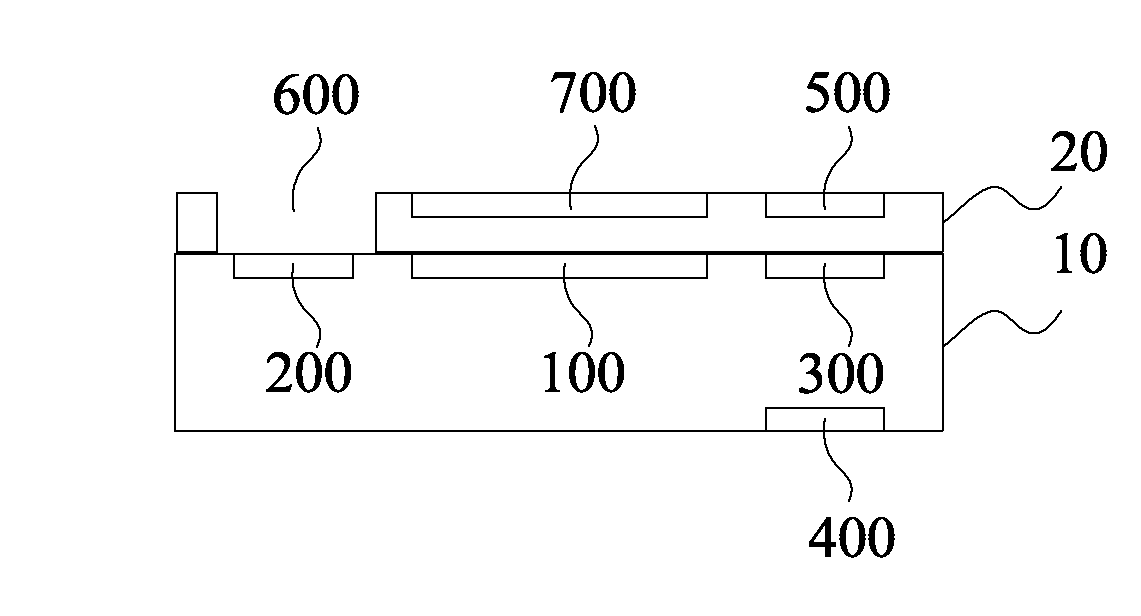
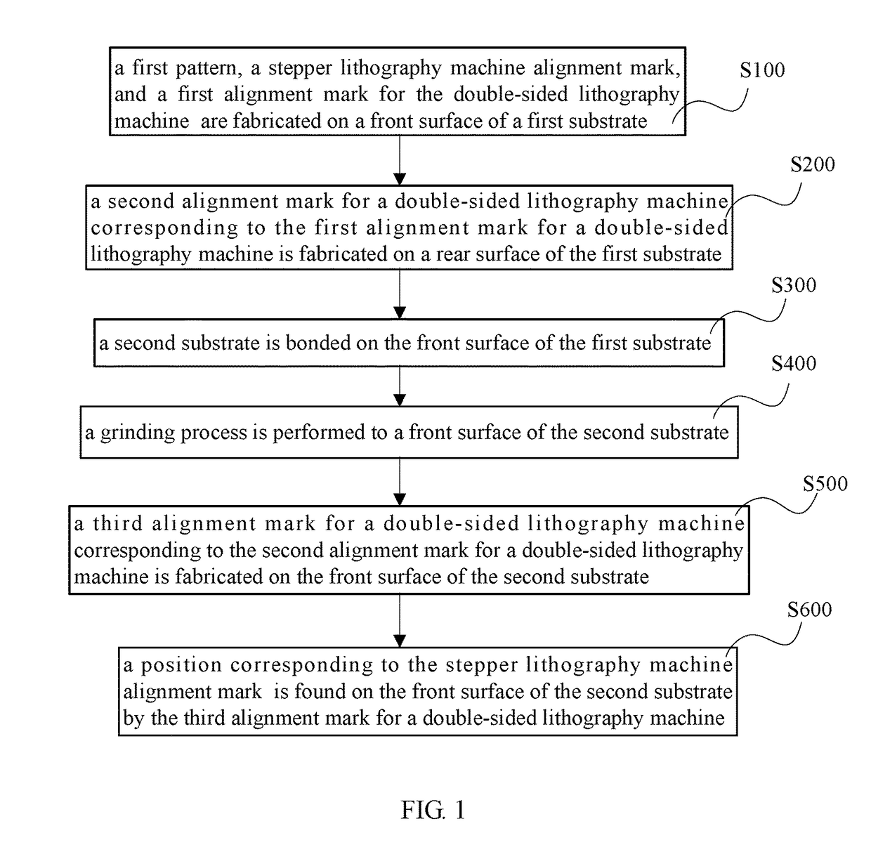
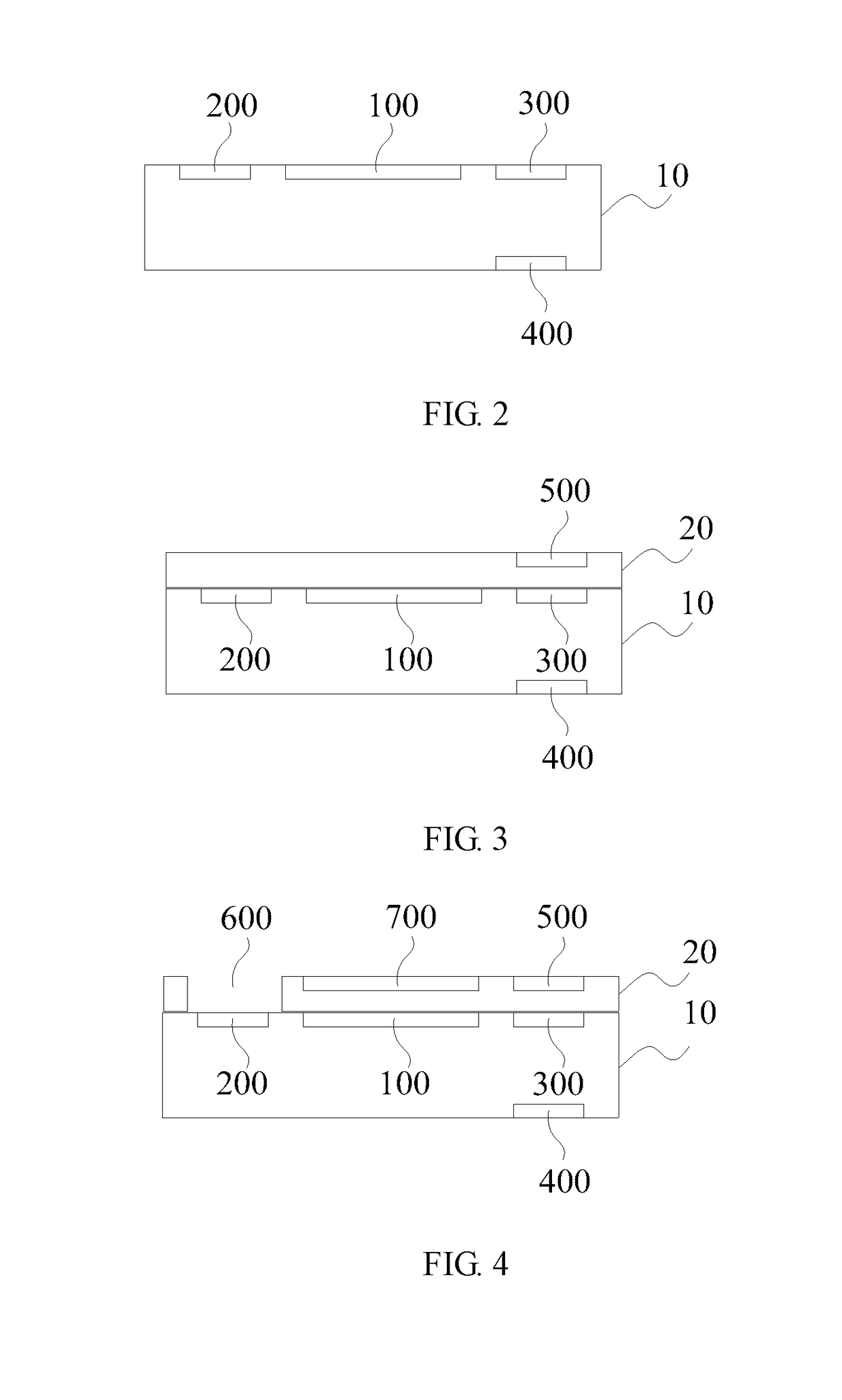
[0014]FIG. 1 is a...


PUM

PropertyMeasurementUnit
thicknessaaaaaaaaaa
dimensionaaaaaaaaaa

Abstract

A positioning method in a microprocessing process of bulk silicon comprises the steps of: fabricating, on a first surface of a first substrate (10), a first pattern (100), a stepper photo-etching machine alignment mark (200) for positioning the first pattern, and a double-sided photo-etching machine first alignment mark (300) for positioning the stepper photo-etching machine alignment mark; fabricating, on a second surface, opposite to the first surface, of the first substrate, a double-sided photo-etching machine second alignment mark (400) corresponding to the double-sided photo-etching machine first alignment mark; bonding a second substrate (20) on the first surface of the first substrate; performing thinning on a first surface of the second substrate; fabricating, on the first surface of the second substrate, a double-sided photo-etching machine third alignment mark (500) corresponding to the double-sided photo-etching machine second alignment mark; and finding, on the first surface of the second substrate by using the double-sided photo-etching machine third alignment mark, a corresponding position of the stepper photo-etching machine alignment mark.

Description

FIELD OF THE INVENTION[0001]The present invention relates to a technical field of semiconductors, and more particularly relates to a positioning method in micromachining process for a bulk silicon.BACKGROUND OF THE INVENTION[0002]MEMS micromachining technology includes a micromachining process for a bulk silicon and a surface micromachining technology. A commonly used micromachining process for a bulk silicon is: first fabricating patterns (such as a deep channel) on one silicon wafer, and then bonding the silicon wafer to another one silicon wafer, performing a grinding to the bonded silicon wafer, and fabricating patterns on a surface of the bonded silicon wafer. The micromachining process for a bulk silicon can manufacture a monocrystalline silicon structure having a greater thickness, and is extensively applied to fields such as an acceleration sensor, a gyroscope, and a microscope. In order to guarantee an alignment between the patterns on surfaces of the upper silicon wafer an...

Claims


Application Information

Patent Timeline
Patent Type & Authority Patents(United States)
IPC IPC(8): H01L21/00B81C3/00
CPCB81C3/004B81C1/00603B81C2203/051B81C1/00B81C3/00G03F9/00H01L21/68
Inventor JING, ERRONG
Owner CSMC TECH FAB2 CO LTD
Features
  • R&D
  • Intellectual Property
  • Life Sciences
  • Materials
  • Tech Scout
  • Unparalleled Data Quality
  • Higher Quality Content
  • 60% Fewer Hallucinations
Learn More