Hybrid chip-on-board LED module with patterned encapsulation

a chip-on-board led module and hybrid technology, applied in the field of light-emitting elements, can solve the problems of loss of absorbed light and corresponding loss of light output efficiency, and achieve the effect of minimal efficiency-reducing absorption and efficient production of desired light outpu

Active Publication Date: 2018-02-27
LUMILEDS
View PDF13 Cites 1 Cited by
  • Summary
  • Abstract
  • Description
  • Claims
  • Application Information

AI Technical Summary

Benefits of technology

[0008]It would be advantageous to provide a hybrid light emitting module in a chip-on-board architecture that is more efficient than conventional chip-on-board modules.
[0011]Accordingly, in embodiments of this invention, the light emitting elements of different colors are paired with encapsulants that efficiently produce a desired light output with minimal efficiency-reducing absorptions. The light emitting elements of light of a particular wavelength that is not intended to be converted by the wavelength conversion material, for example, may be encapsulated with a phosphor-free encapsulant, while light emitting elements of light that is intended to be converted may be encapsulated with a phosphor, or phosphor mix, that efficiently converts some or all of the light to a desired wavelength or set of wavelengths.

Problems solved by technology

The applicants have recognized that although each phosphor may efficiently absorb light of a first range of wavelengths and emit light of a desired second range of wavelengths, the phosphor may also absorb light of other wavelengths and not emit light at all, or emit a minimal amount of light at a third, perhaps undesired, range of wavelengths, resulting in a loss of the absorbed light, and a corresponding loss of light output efficiency.

Method used


Image

  • Hybrid chip-on-board LED module with patterned encapsulation
  • Hybrid chip-on-board LED module with patterned encapsulation
  • Hybrid chip-on-board LED module with patterned encapsulation

Examples


Embodiment Construction

[0019]In the following description, for purposes of explanation rather than limitation, specific details are set forth such as the particular architecture, interfaces, techniques, etc., in order to provide a thorough understanding of the concepts of the invention. However, it will be apparent to those skilled in the art that the present invention may be practiced in other embodiments, which depart from these specific details. In like manner, the text of this description is directed to the example embodiments as illustrated in the Figures, and is not intended to limit the claimed invention beyond the limits expressly included in the claims. For purposes of simplicity and clarity, detailed descriptions of well-known devices, circuits, and methods are omitted so as not to obscure the description of the present invention with unnecessary detail.

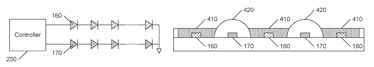
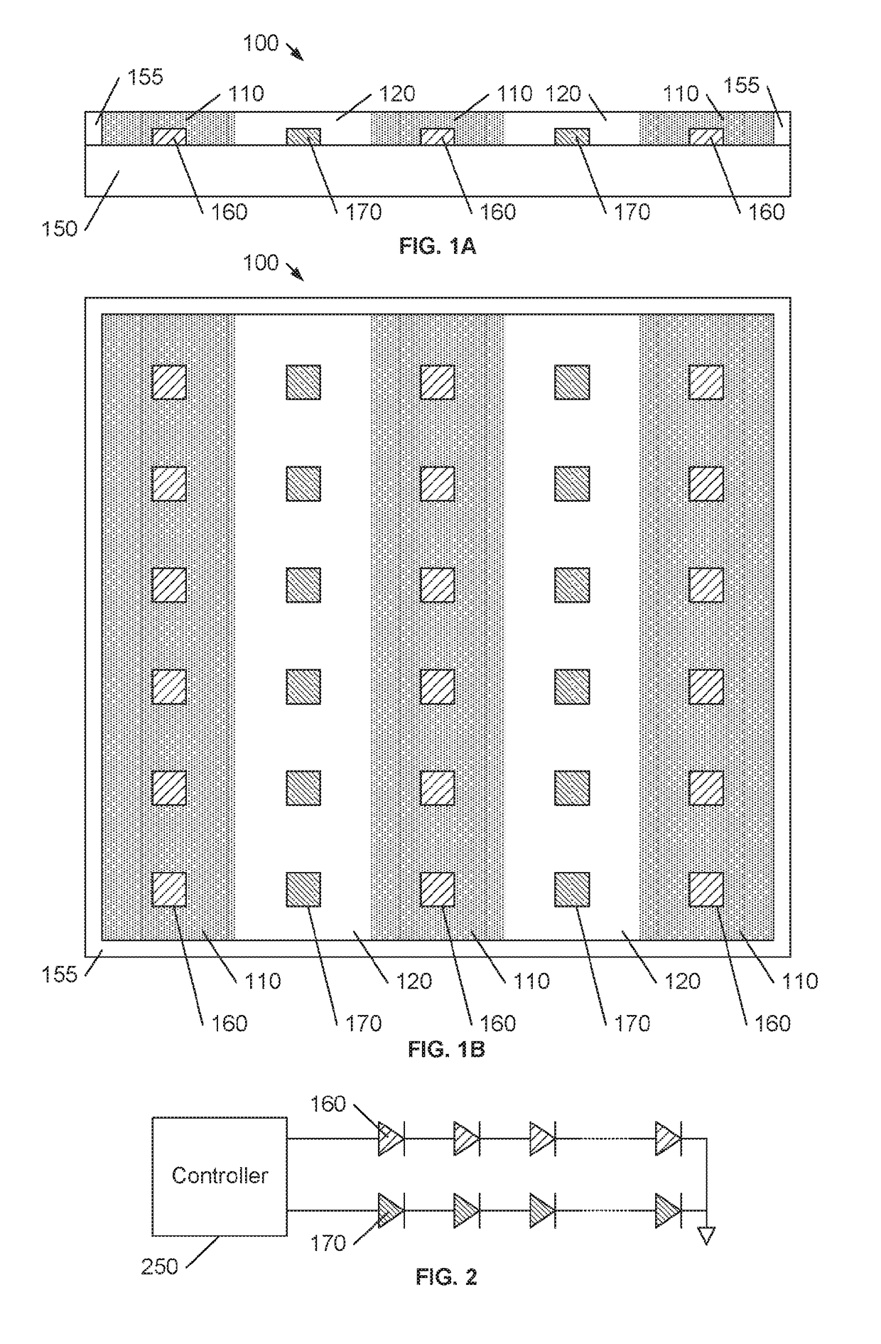
[0020]FIG. 1A illustrates a profile view and FIG. 1B illustrates a top view of an example light emitting module 100 that includes different enca...


PUM


Abstract

Different wavelength conversion materials, or different concentrations of a wavelength conversion material are used to encapsulate the light emitting elements of different colors of a hybrid light emitting module. In an embodiment of this invention, second light emitting elements (170) of a particular color are encapsulated with a transparent second encapsulant (120;420;520), while first light emitting elements (160) of a different color are encapsulated with a wavelength conversion first encapsulant (110;410;510). In another embodiment of this invention, a particular second set of second and third light emitting elements (170,580) of different colors is encapsulated with a different encapsulant than another first set of first light emitting elements (160).

Description

CROSS-REFERENCE TO RELATED APPLICATIONS[0001]The present application is a § 371 application of International Application No. PCT / IB2014 / 064070 filed on Aug. 26, 2014 and entitled “HYBRID CHIP-ON-BOARD LED MODULE WITH PATTERNED ENCAPSULATION,” which claims priority to U.S. Provisional Patent Application No. 61 / 929,530 filed Jan. 21, 2014. Both PCT / IB2014 / 064070 and 61 / 929,530 are incorporated herein.[0002]This invention was made with U.S. Government support under Contract No. DE-EE0005099 awarded by the Department of Energy (DOE). The Government has certain rights in this invention.FIELD OF THE INVENTION[0003]This invention relates to the field of light emitting elements, and in particular to a hybrid (multiple light emitting elements of different colors) LED module that includes a patterned encapsulation that provides different wavelength conversion elements for different colors.BACKGROUND OF THE INVENTION[0004]With the increased demand for high-output semiconductor light emitting d...

Claims


Application Information

Patent Timeline
Patent Type & Authority Patents(United States)
IPC IPC(8): F21V9/00H05B33/08H05B37/02H01L33/54H01L25/075H01L33/50H01L33/52F21V9/40H05B44/00
CPCH01L33/508H01L25/0753H01L33/54H05B33/0845H05B37/0209H01L33/50H01L33/52H01L2933/0091H01L2924/0002H01L2933/005H01L2933/0041H01L2924/00H05B47/10H05B45/10F21Y2105/14F21Y2115/10H01L33/502
Inventor SOER, WOUTER ANTHONHELBING, RENEHUANG, GUAN
Owner LUMILEDS
Why Eureka
Try Eureka