Thermal processing method and thermal processing apparatus through light irradiation

a technology of thermal processing apparatus and electronic substrate, which is applied in the direction of vacuum evaporation coating, semiconductor wafer testing/measurement, and test/measurement of semiconductor/solid-state devices, etc., can solve the problems of uniform temperature history, potential damage of semiconductor wafers, and difficulty in favorable device formation, etc., to achieve the effect of improving the heating accuracy of the susceptor

Active Publication Date: 2018-03-20
DAINIPPON SCREEN MTG CO LTD
View PDF7 Cites 3 Cited by
  • Summary
  • Abstract
  • Description
  • Claims
  • Application Information

AI Technical Summary

Problems solved by technology

In this process, an annealing time of several seconds or longer allows the implanted impurities to deeply diffuse by heat to have a junction depth much larger than required, potentially causing difficulties in favorable device formation.
This causes such a problem that a temperature history is ununiform among a plurality of semiconductor wafers included in the lot.
When a semiconductor wafer supported by the susceptor at low temperature is irradiated with flash light, wafer warpage occurs in some cases because of a temperature difference between the susceptor and the semiconductor wafer, and as a result, the semiconductor wafer is potentially damaged.
However, in such dummy running, a dummy wafer that is not a processing target is consumed, and it takes a considerable time to perform the flash heating processing on about 10 dummy wafers, preventing efficient operation of the flash lamp anneal apparatus.

Method used


Image

  • Thermal processing method and thermal processing apparatus through light irradiation
  • Thermal processing method and thermal processing apparatus through light irradiation
  • Thermal processing method and thermal processing apparatus through light irradiation

Examples


first preferred embodiment

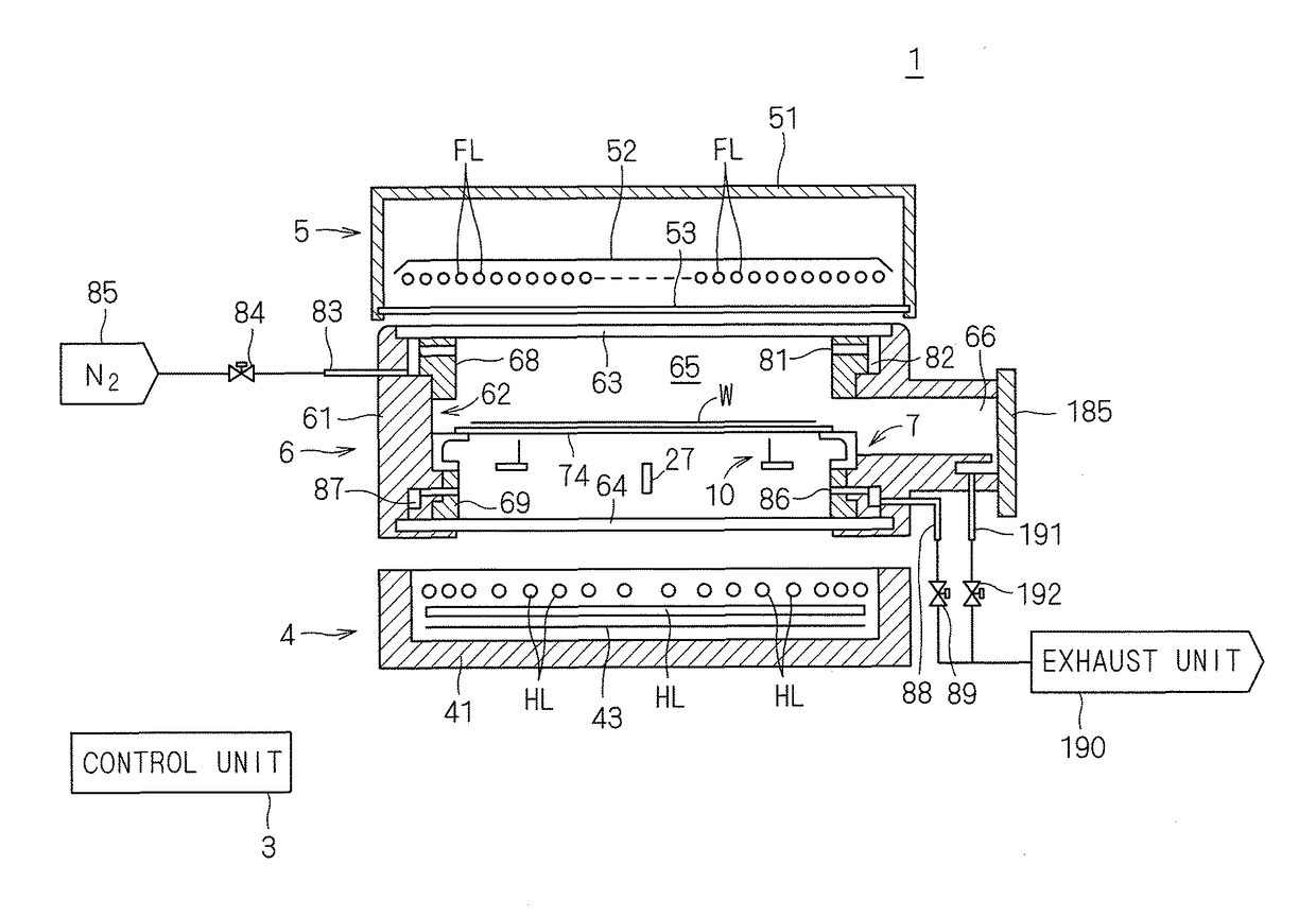
[0036]FIG. 1 is a vertical sectional view illustrating the configuration of a thermal processing apparatus 1 according to the present invention. The thermal processing apparatus 1 according to the present preferred embodiment is a flash lamp annealing apparatus configured to heat a semiconductor wafer W, as a substrate, in a circular disk shape by irradiating the semiconductor wafer W with flash light. The size of the semiconductor wafer W to be processed is not particularly limited, but is, for example, φ 300 mm or φ 450 mm. Impurities are implanted in the semiconductor wafer W before being transferred into the thermal processing apparatus 1, and activation processing of the implanted impurities is executed through heating processing by the thermal processing apparatus 1. In FIG. 1 and the following drawings, the dimension of each component and the number thereof are exaggerated or simplified as necessary to facilitate understanding.

[0037]The thermal processing apparatus 1 includes...

second preferred embodiment

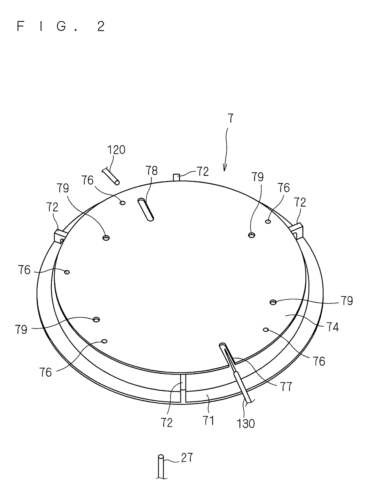
[0096]The following describes a second preferred embodiment of the present invention. The entire schematic configuration of a thermal processing apparatus and a procedure of processing the semiconductor wafer W according to the second preferred embodiment are substantially same as those of the first preferred embodiment, but the number of radiation thermometers configured to measure the temperature of the susceptor 74 is different from the first preferred embodiments. Although the single radiation thermometer 27 is provided to measure temperature at a central part of the susceptor 74 in the first preferred embodiment, a plurality of radiation thermometers are provided to measure temperature at a plurality of places on the susceptor 74 in the second preferred embodiment.

[0097]Specifically, in the second preferred embodiment, a total of three radiation thermometers of a radiation thermometer configured to measure temperature at a central part of the susceptor 74, a radiation thermomet...


PUM

PropertyMeasurementUnit
sizeaaaaaaaaaa
sizeaaaaaaaaaa
temperatureaaaaaaaaaa

Abstract

A susceptor is preheated through light irradiation by a halogen lamp before the first semiconductor wafer of a lot as a processing target is transferred into a chamber. The temperature of the susceptor is measured by a radiation thermometer. A control unit is configured to control the output of the halogen lamp so that the temperature of the susceptor reaches a stable temperature based on a result of the measurement of the temperature of the susceptor by the radiation thermometer. The stable temperature of the susceptor is the temperature of the susceptor when the temperature of the susceptor is risen to a constant temperature by continuously performing light irradiation heating on a plurality of semiconductor wafers in the chamber without heating the susceptor.

Description

BACKGROUND OF THE INVENTION[0001]Field of the Invention[0002]The present invention relates to a thermal processing method and thermal processing apparatus of heating a thin-plate fine electronic substrate (hereinafter simply referred to as a “substrate”) such as a semiconductor wafer to which impurities are introduced, by irradiating the substrate with light.[0003]Description of the Background Art[0004]In a process of manufacturing a semiconductor device, impurity introduction is a process necessary for forming a p-n junction in a semiconductor wafer. Currently, a typical impurity introduction is achieved by an ion implantation technique and a subsequent annealing technique. The ion implantation technique is a technology in which impurity elements such as boron (B), arsenic (As), and phosphorus (P) are ionized to collide onto a semiconductor wafer with a high acceleration voltage and physically perform impurity implantation. Implanted impurities are activated through anneal processi...

Claims


Application Information

Patent Timeline
Patent Type & Authority Patents(United States)
IPC IPC(8): H01L21/00H01L21/66C23C14/02C23C14/48H01L21/324H01L21/67H01L21/225
CPCH01L22/20C23C14/02C23C14/48H01L21/67248H01L21/324H01L21/67115H01L21/2253
Inventor ONO, YUKIO
Owner DAINIPPON SCREEN MTG CO LTD
Why Eureka
Try Eureka