Electro-optic device, eletro-optic unit, and electronic apparatus

a technology of electro-optic devices and electronic devices, applied in microelectromechanical systems, instruments, color television details, etc., can solve the problems of reducing the life of electro-optic devices, the thermal conductivity of sealing resin itself is low, and the chip temperature cannot be sufficiently suppressed

Active Publication Date: 2018-04-03
SEIKO EPSON CORP
View PDF4 Cites 2 Cited by
  • Summary
  • Abstract
  • Description
  • Claims
  • Application Information

AI Technical Summary

Benefits of technology

[0008]According to this aspect of the invention, even if the temperature of the chip rises, the heat of the chip can be released to the metal member disposed in the interconnection board. Further, since the interconnection board is provided with the through hole extending so as to have contact with the metal member, the heat of the metal member can be released with the air flowing through the first through hole. Therefore, since the heat of the chip can efficiently be released, the rise in temperature of the chip can be suppressed. Therefore, it is possible to prevent the deterioration of the reliability of the electro-optic device.
[0009]In the aspect of the invention, it is preferable that the interconnection board is provided with a second through hole extending from the third surface to the fourth surface, and having contact with the metal member from an opposite side to a side from which the first through hole has contact with the metal member. According to such a configuration, the heat of the metal member can be released by the air flowing through the first through hole and the second through hole. Therefore, since the rise in temperature of the chip can be suppressed, the deterioration of the reliability of the electro-optic device can be prevented.
[0010]In the aspect of the invention with this configuration, it is preferable that the chip is located so as to overlap the metal member. According to such a configuration, it is possible to efficiently release the heat of the chip to the metal member.
[0011]In the aspect of the invention, it is preferable that the chip has contact with the metal member directly or via an adhesive layer. According to such a configuration, it is possible to efficiently release the heat of the chip to the metal member.
[0014]In an electro-optic unit having the electro-optic device to which the invention is applied, it is preferable to include a blower adapted to feed air toward the third surface. According to such a configuration, since the heat of the metal member can efficiently be released using the air passing through the first through hole, it is possible to prevent the deterioration of the reliability of the electro-optic device and so on.

Problems solved by technology

Such rise in temperature of the chip causes a false operation and a decrease in life of the electro-optic device, and is therefore undesirable.
However, even if the heat-transfer efficiency from the cover and so on to the sealing resin is improved with the configuration described in Document 1, the thermal conductivity of the sealing resin itself is low, and therefore, there is a problem that the rise in temperature of the chip cannot sufficiently be suppressed.

Method used


Image

  • Electro-optic device, eletro-optic unit, and electronic apparatus
  • Electro-optic device, eletro-optic unit, and electronic apparatus
  • Electro-optic device, eletro-optic unit, and electronic apparatus

Examples


Embodiment Construction

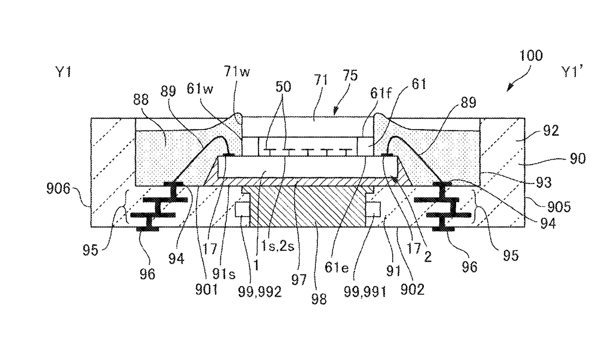
[0028]An embodiment of the invention will be described with reference to the accompanying drawings. It should be noted that in the following description, a projection-type display device will be explained as an electronic apparatus to which the invention is applied. Further, in the drawings referred to in the following description, the scale ratios of the layers and the members are made different from each other in order to provide the layers and the members with the sizes in a recognizable range on the drawings. Although the number of the mirrors and so on shown in the drawings is set so as to provide the size in the recognizable range on the drawings, it is also possible to provide a larger number of mirrors than the number of mirrors shown in the drawings.

Projection-Type Display Device as Electronic Apparatus

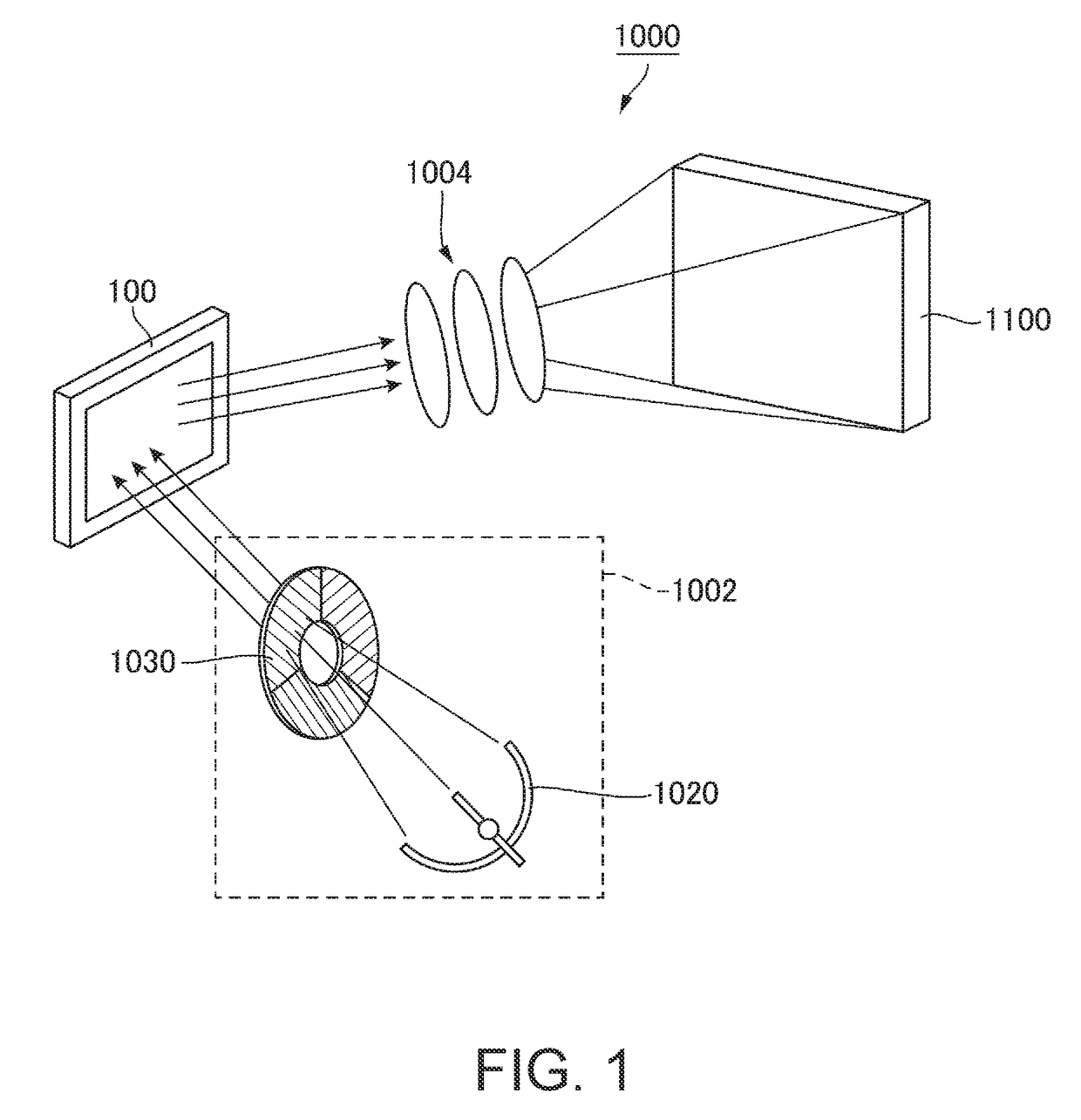
[0029]FIG. 1 is an explanatory diagram schematically showing an example of an optical system provided to a projection-type display device to which the invention is applied. T...


PUM


Abstract

An electro-optic device includes an interconnection board provided with an internal terminal, and a chip mounted on the interconnection board, and the chip is provided with a mirror, a drive element, and a chip-side terminal electrically connected to the drive element. The interconnection board includes a first surface on which an internal terminal is disposed, a second surface located on an opposite side to the first surface, a third surface connecting the first surface and the second surface to each other, and a fourth surface located on an opposite side to the third surface. The interconnection board is provided with a metal member exposed on the first surface and the second surface, and through holes (a first through hole and a second through hole) extending from the third surface to the fourth surface and having contact with the metal member.

Description

[0001]The entire disclosure of Japanese Patent Application No. 2016-065206, filed Mar. 29, 2016 is expressly incorporated by reference herein.BACKGROUND1. Technical Field[0002]The present invention relates to an electro-optic device equipped with a mirror, an electro-optic unit, and an electronic device.2. Related Art[0003]As an electronic apparatus, there has been known, for example, a projection-type display device, which modulates the light emitted from a light source using a plurality of mirrors (micro mirrors) of an electro-optic device called a digital mirror device (DMD), and then projects the modulated light in an enlarged manner using a projection optical system. Such an electro-optic device has a chip provided with mirrors and drive elements for driving the mirrors, and an interconnection board on which the chip is mounted, and when the electro-optic device operates, the chip itself generates heat. Further, in the case of disposing a light-transmitting cover for covering t...

Claims


Application Information

Patent Timeline
Patent Type & Authority Patents(United States)
IPC IPC(8): G02B26/08G03B21/00
CPCG03B21/008G02B26/0833G02B26/0841B81B7/0067B81B7/0093B81B2201/042H04N9/3114H04N9/3144
Inventor UCHIYAMA, SUGURUTAKAHASHI, KOSUKE
Owner SEIKO EPSON CORP
Why Eureka
Try Eureka