Self-aligned block patterning with density assist pattern

a technology of assist pattern and self-aligning block, which is applied in the direction of photomechanical treatment, semiconductor devices, instruments, etc., can solve the problems of non-uniform mask pattern transfer, unwanted pattern being printed on the wafer, and mask uniformity issue, so as to improve uniformity and improve uniformity. uniform

Active Publication Date: 2018-04-10
SAMSUNG ELECTRONICS CO LTD
View PDF1 Cites 27 Cited by
  • Summary
  • Abstract
  • Description
  • Claims
  • Application Information

AI Technical Summary

Benefits of technology

[0009]The mask layouts provided in the present invention may have a pattern density of 30% or greater, preferably 40% or greater, thus the masks with the mask layouts and the metal lines fabricated with the masks of the present invention may have better uniformity. When EUV lithography is used, the EUV masks with the mask layouts of the present invention may have better uniformity and lower defect level, and metal lines fabricated with the EUV masks may also have better uniformity and lower defect level.

Problems solved by technology

Current issue for block patterning is very low density, it causes a mask uniformity issue, and the non-uniform mask pattern is transferred to wafer.
In case of EUV mask, there are natural defects on the blank, and the defects may cause unwanted pattern being printed on the wafer.
Lower pattern density increases the probability of fabricating defective EUV mask.
In addition, photoresists used in fabricating masks are usually positive tone, lower pattern density will require longer E-beam writing time, which not only hurts throughput also causes critical dimension (CD) errors.

Method used


Image

  • Self-aligned block patterning with density assist pattern
  • Self-aligned block patterning with density assist pattern
  • Self-aligned block patterning with density assist pattern

Examples


Embodiment Construction

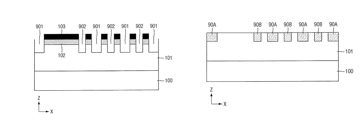
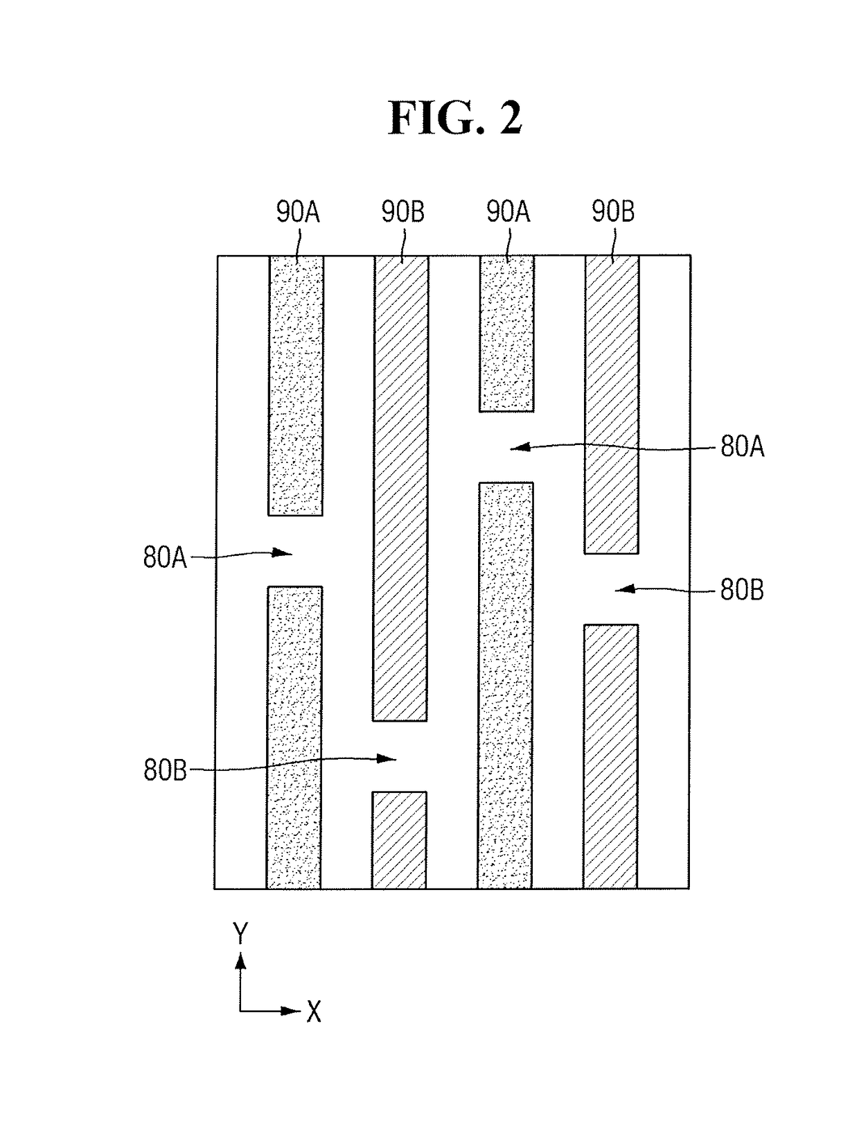
[0028]This invention relates generally to a method of generating mask layouts including density assist patterns for self-aligned block (SAB) patterning process and a method of using masks with the layouts thereof for the SAB patterning process. Specifically, the present invention relates to a method of generating SAB patterning mask layouts which include density assist patterns to increase pattern density, so that the masks with the layouts will have better uniformity. Low pattern density in mask may cause uniformity issue. For EUV mask, higher pattern density may also reduce the number of natural defects of the blank, because the defects may be covered by the absorber. Thus, higher pattern density will not only increase uniformity, but also reduce defect level in EUV mask. Usually, the mask features are linearly imaged onto a wafer. As a result, metal lines fabricated by the SAB patterning process using the above described masks with higher pattern density (e.g., ≥30%) will have be...


PUM


Abstract

A method of generating mask layouts for self-aligned block patterning is provided. Metal line patterns to be formed on a semiconductor substrate is identified. A mandrel mask layout for first mask based on the metal line patterns is generated in view of a self-aligned double patterning (SADP) process for forming a plurality of mandrels on the semiconductor substrate. The mandrel mask layout may include a plurality of mandrel patterns. A non-mandrel block mask layout for second mask is generated based on the mandrel mask layout for cutting metal lines formed under gaps between spacers in non-mandrel area on the semiconductor substrate. The non-mandrel block mask layout may include a plurality of first block patterns and a plurality of first density assist patterns. A mandrel block mask layout for third mask is generated based on the mandrel mask layout for cutting metal lines formed under mandrel area on the semiconductor substrate.

Description

CROSS-REFERENCE TO RELATED APPLICATION[0001]This application claims the benefit under 35 U.S.C. § 119(e) to U.S. Provisional Patent Application No. 62 / 430,056, filed on Dec. 5, 2016 in the United States Patent & Trademark Office, the disclosure of which is incorporated by reference herein in its entirety.TECHNICAL FIELD[0002]This invention relates generally to a method of generating mask layouts including density assist patterns for self-aligned block patterning process, a method of using masks with the layouts, and a method of manufacturing an integrated circuit using masks with the layouts.DISCUSSION OF RELATED ART[0003]In the fabrication of integrated circuits, lithography is used to generate pattern structures on the semiconductor and various materials for the construction of the desired circuit structures. A continuing demand in view of the ever-increasing desire in the semiconductor industry for higher circuit density in microelectronic devices has prompted lithographic engine...

Claims


Application Information

Patent Timeline
Patent Type & Authority Patents(United States)
IPC IPC(8): H01L21/033H01L21/768H01L21/311H01L21/308
CPCH01L21/76897H01L21/76816H01L21/3088H01L21/3086H01L21/31144H01L21/0338H01L21/0337H01L21/3083H01L21/76877G03F7/168H01L21/0274H01L27/0611
Inventor KIM, SEONG JONG
Owner SAMSUNG ELECTRONICS CO LTD
Why Eureka
Try Eureka