Refresh control circuit for target refresh operation of semiconductor memory device, and operating method thereof

a control circuit and memory device technology, applied in the field of semiconductor memory device refresh control circuit, can solve the problems of row hammering effect, data loss, and memory cell data being deteriorated within a shorter time than the refresh term, and achieve the effect of preventing data loss of memory cells

Active Publication Date: 2018-04-24
SK HYNIX INC
View PDF15 Cites 64 Cited by
  • Summary
  • Abstract
  • Description
  • Claims
  • Application Information

AI Technical Summary

Benefits of technology

[0013]Embodiments of the present invention are directed to providing a refresh control circuit capable of performing a target refresh operation capable of preventing data loss of memory cells due to the Row Hammering effect, a semiconductor memory device employing the refresh control circuit, and an operating method of the semiconductor memory device. The target refresh operation may be in addition to a normal refresh operation.

Problems solved by technology

However, because of a current leak due to a PN junction of a transistor, the initial amount of charges that are stored in a capacitor may gradually disappear, thereby causing data loss.
However, when the amount of charges stored in a memory cell is affected by the active-precharge of a word line that is disposed adjacent to a word line coupled to the memory cell, the data of the memory cell may be deteriorated within a shorter time than the refresh term.
The Row Hammering effect may be a serious concern, especially for high density semiconductor memory devices due to the increased proximity of neighboring word lines.
Normal refresh operations which sequentially refresh the plurality of word lines in a memory device when a refresh command is inputted do not specifically address data loss of memory cells due to the Row Hammering effect.

Method used


Image

  • Refresh control circuit for target refresh operation of semiconductor memory device, and operating method thereof
  • Refresh control circuit for target refresh operation of semiconductor memory device, and operating method thereof
  • Refresh control circuit for target refresh operation of semiconductor memory device, and operating method thereof

Examples


Embodiment Construction

[0032]Exemplary embodiments of the present invention will be described below in more detail with reference to the accompanying drawings. The present invention may, however, be embodied in different forms and should not be construed as limited to the embodiments set forth herein. Rather, these embodiments are provided so that this disclosure will be thorough and complete and will fully convey the scope of the present invention to those skilled in the art. Throughout the disclosure, like reference numerals refer to like parts throughout the various figures and embodiments of the present invention.

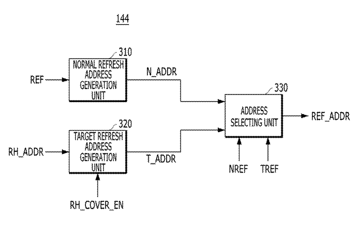
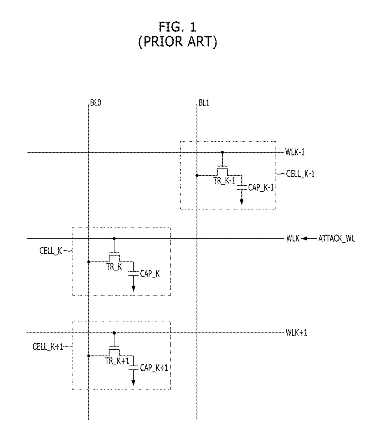
[0033]Hereafter, a target refresh operation of additionally refreshing a word line corresponding to a target address is described by referring to the accompanying drawings. For the sake of convenience in description, a structure related to rows is mainly illustrated in the drawings.

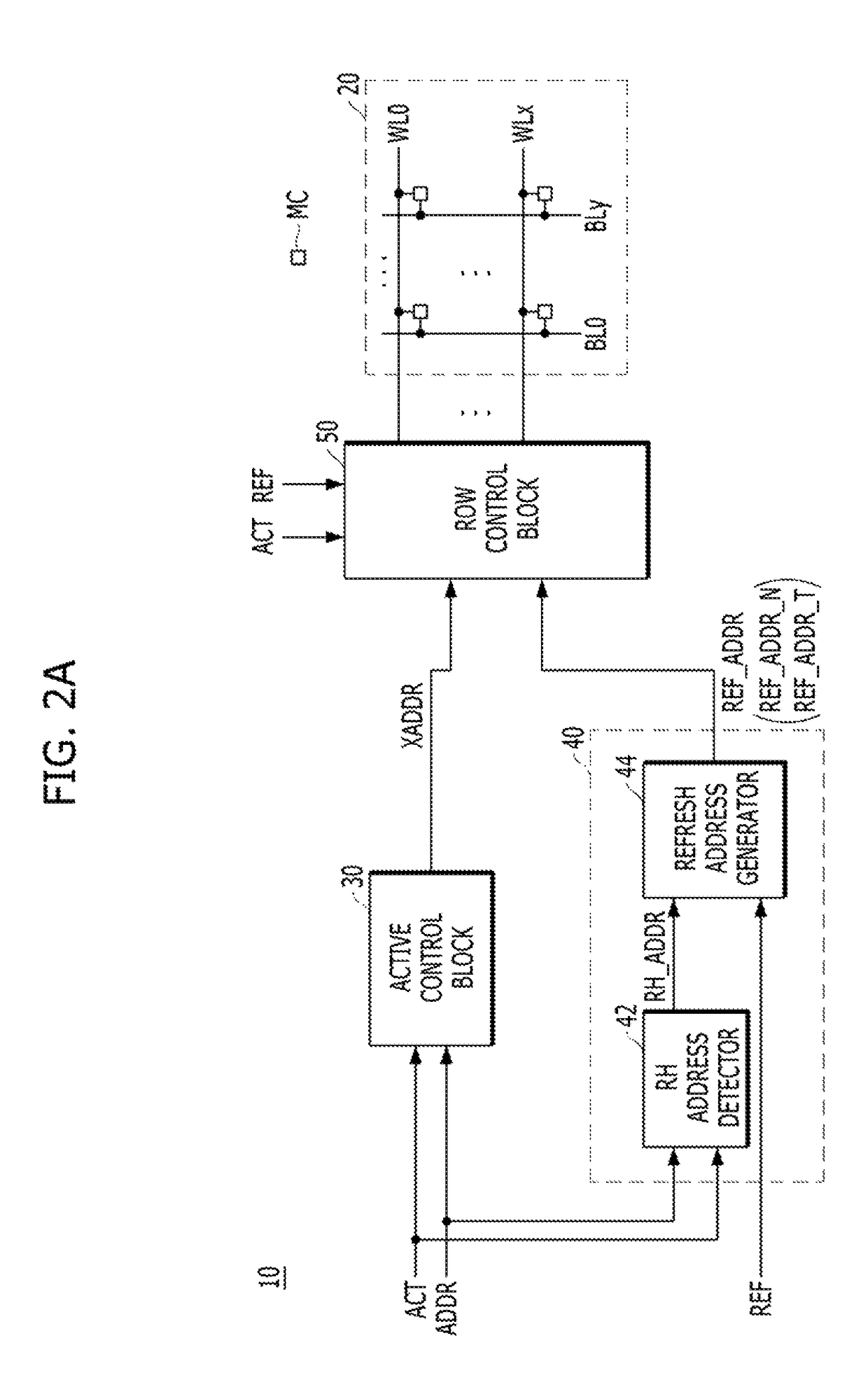
[0034]FIG. 2A is a block diagram illustrating a semiconductor memory device 10 that performs a target refresh op...


PUM


Abstract

A semiconductor memory device may include: a memory cell region including a plurality of memory cells coupled between a plurality of word lines and a plurality of bit lines; and a refresh control block suitable for performing a first refresh operation onto the plurality of the word lines in response to a refresh signal, counting the number of active signals that are inputted between at least two neighboring refresh signals and when the counted number of the active signals is equal to or greater than a reference number, performing a second refresh operation onto a word line corresponding to a target address.

Description

CROSS-REFERENCE TO RELATED APPLICATIONS[0001]The present application claims priority of Korean Patent Application No. 10-2016-0106908, filed on Aug. 23, 2016, which is incorporated herein by reference in its entirety.BACKGROUND[0002]1. Field[0003]Exemplary embodiments of the present invention relate generally to a semiconductor design technology, and more particularly, to a refresh control circuit for a semiconductor memory device that is capable of performing a target refresh operation.[0004]2. Description of the Related Art[0005]A memory device may typically include a plurality of memory cells for storing data in the form of stored charges. Each memory cell may typically include a capacitor that stores charges (i.e., data) and a transistor that serves as a switch controlling the flow of charges to and from the capacitor. Whether a data is in a ‘high’ logic level (i.e., a logic value ‘1’) or a ‘low’ logic level (i.e., a logic value ‘0’) is decided based on whether there are charges...

Claims


Application Information

Patent Timeline
Patent Type & Authority Patents(United States)
IPC IPC(8): G11C8/00G11C11/406G11C11/4076G11C11/4078
CPCG11C11/4078G11C11/40611G11C11/4076G11C11/40622G11C2211/4065G11C11/4085G06F2212/7211
Inventor KIM, JUNG-HYUN
Owner SK HYNIX INC
Why Eureka
Try Eureka