Method for manufacturing light extraction substrate for organic light-emitting element, light extraction substrate for organic light-emitting element, and organic light-emitting element comprising same

a technology of organic light-emitting elements and manufacturing methods, which is applied in the direction of basic electric elements, electrical devices, semiconductor devices, etc., can solve the problems of reducing the overall luminous efficiencyaffecting forming fine cracks in the coating film. , to achieve the effect of improving the light extraction efficiency and luminance uniformity reducing the fabrication cost of the oled devi

Active Publication Date: 2018-05-01
SAMSUNG CORNING PRECISION MATERIALS CO LTD
View PDF13 Cites 1 Cited by
  • Summary
  • Abstract
  • Description
  • Claims
  • Application Information

AI Technical Summary

Benefits of technology

[0031]According to the present disclosure, an electrode supposed to function as an auxiliary electrode of an OLED device is manufactured by forming a random network structure by controlling the shape of cracks formed, without additional processing, due to the difference in coefficients of thermal expansion (CTE) between a mixture and a base substrate during contraction of the mixture for forming a matrix layer and then depositing metal in the cracks. When applied to the OLED device, it is possible to improve the light extraction efficiency and luminance uniformity of the OLED device and enable the OLED device to operate at a low voltage. Accordingly, the present disclosure is applicable to the OLED device having a large area.
[0032]In addition, according to the present disclosure, the electrode is formed by filling cracks that are formed without additional processing. The electrode can be formed in a simpler manner than a conventional process in which the auxiliary electrode of the OLED device is formed by photolithography, thereby reducing fabrication costs of the OLED device.
[0033]Furthermore, according to the present disclosure, a conductive film supposed to function as a transparent electrode of an OLED device is formed to cover the surface of the auxiliary electrode formed in the cracks and the surface of the matrix layer. Then, the surface of the matrix layer, the roughness of which is increased by the occurrence of the cracks, can be planarized. This can consequently remove an additional process for forming a planarization layer, thereby reducing fabrication costs of the OLED device.
[0034]In addition, according to the present disclosure, when the auxiliary electrode is formed by filling the cracks formed in the matrix layer, the probability that light, wave-guided sideways from the inside of the matrix layer, will arrive at and be reflected from the auxiliary electrode formed from metal is increased. This can consequently disturb a waveguide mode, thereby leading to an improvement in the light extraction efficiency.

Problems solved by technology

This may consequently lower light extraction efficiency, thereby lowering the overall luminous efficiency of the OLED device, which is problematic.
However, due to volumetric contraction caused by the crystallization of the sol of the binder material during the firing operation and the process of relieving stress caused by the difference in coefficients of thermal expansion (CTE) between the substrate and the binder material, fine cracks may be formed in the coating film.
Since the cracks increase the surface roughness of the coating film while reducing the bonding force of the coating film, the top surface of the coating film must be additionally coated with a planarization film, thereby incurring the cost of additional processing, which is problematic.
However, when the auxiliary electrode is formed in such a photolithographic process, the cost of processing may be significantly increased, which is problematic.
The electrical properties of the auxiliary electrode formed by such a printing method are inferior to those of auxiliary electrodes formed by deposition.

Method used


Image

  • Method for manufacturing light extraction substrate for organic light-emitting element, light extraction substrate for organic light-emitting element, and organic light-emitting element comprising same
  • Method for manufacturing light extraction substrate for organic light-emitting element, light extraction substrate for organic light-emitting element, and organic light-emitting element comprising same
  • Method for manufacturing light extraction substrate for organic light-emitting element, light extraction substrate for organic light-emitting element, and organic light-emitting element comprising same

Examples


Embodiment Construction

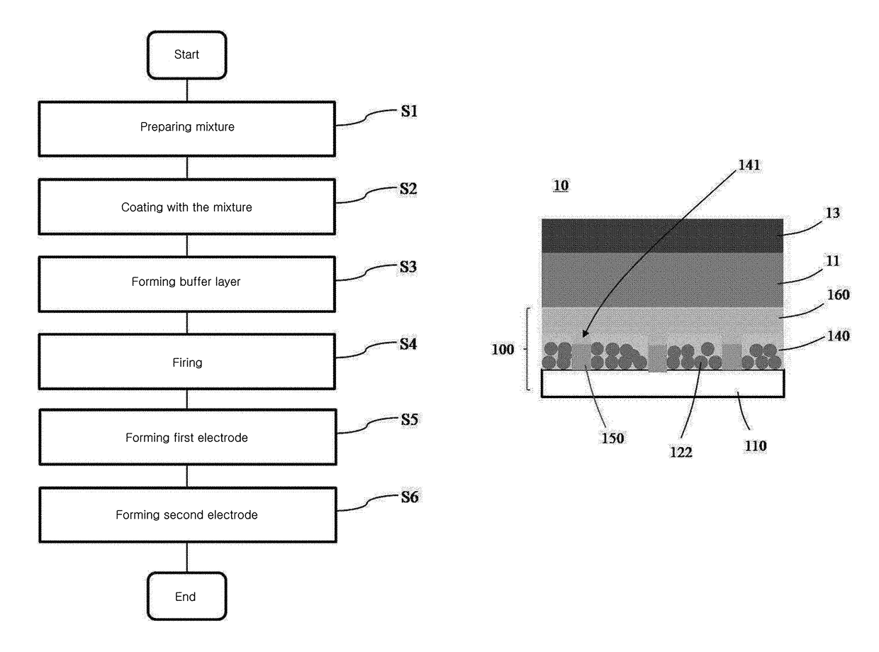
[0038]Hereinafter, a method of manufacturing a light extraction substrate for an organic light-emitting device or an organic light-emitting diode (OLED) device, a light extraction substrate for an OLED device, and an OLED device including the same according to exemplary embodiments will be described in detail with reference to the accompanying drawings.

[0039]In the following description, detailed descriptions of known functions and components incorporated herein will be omitted in the case in which the subject matter of the present disclosure may be rendered unclear by the inclusion thereof.

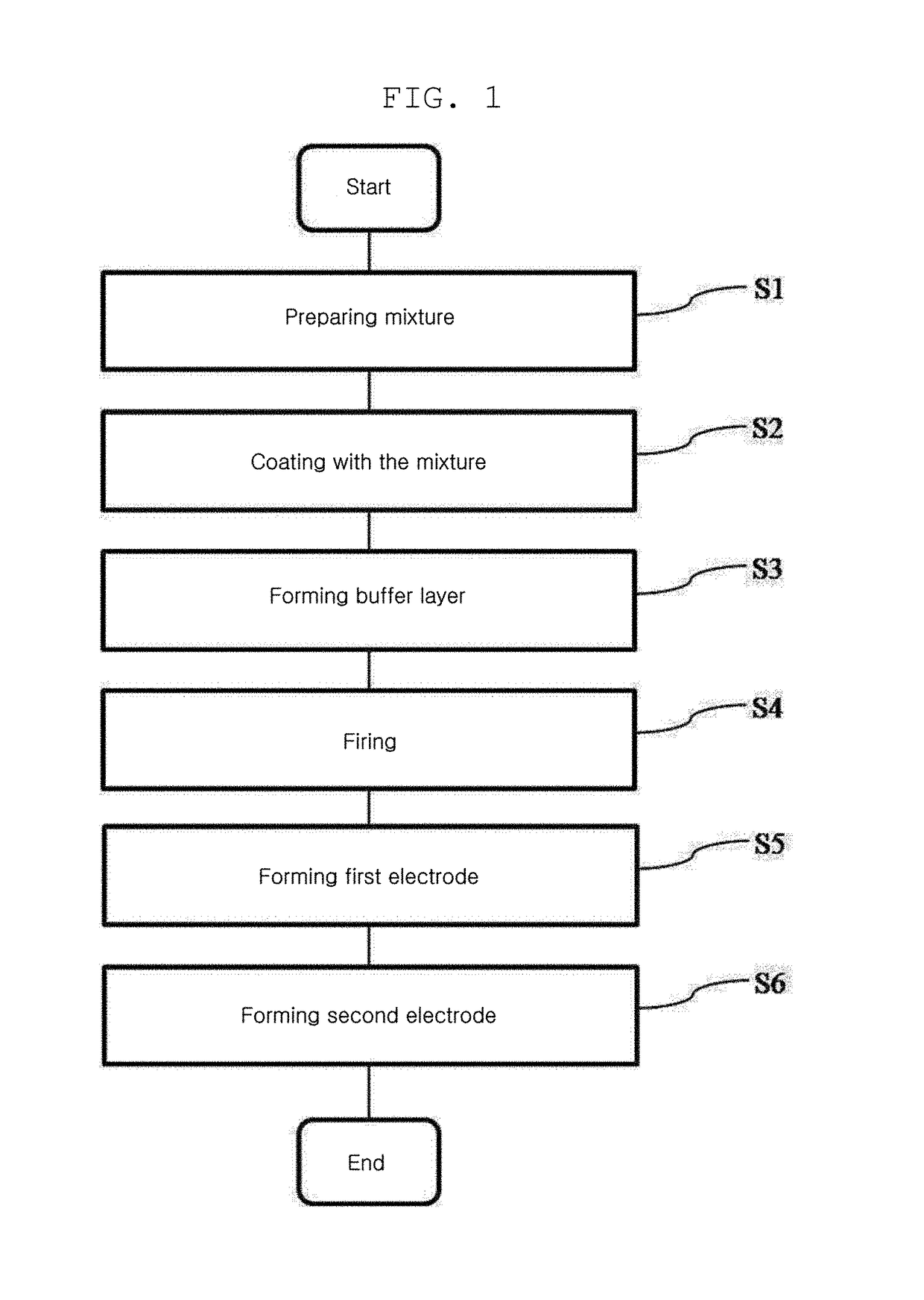
[0040]A method of manufacturing a light extraction substrate for an organic light-emitting device or an OLED device according to an exemplary embodiment is a method of manufacturing a light extraction substrate (100 in FIG. 9) that is disposed on a path, along which light emitted by an OLED of an OLED device (10 in FIG. 9) exits, to function as a route through which light emitted by the OLED can ...


PUM


Abstract

The present invention relates to a method for manufacturing a light extraction substrate for an organic light-emitting element, a light extraction substrate for an organic light-emitting element and an organic light-emitting element comprising the same and, more specifically, to: a method for manufacturing a light extraction substrate for an organic light-emitting element, the method being capable of improving light extraction efficiency of the organic light-emitting element and also increasing luminance uniformity; a light extraction substrate for an organic light-emitting element; and an organic light-emitting element comprising the same. To this end, the present invention provides a method for manufacturing a light extraction substrate for an organic light-emitting element, comprising: a mixture preparation step of preparing a mixture by mixing a plurality of scattering particles with an inorganic binder; a mixture coating step of coating the mixture on a base substrate; a buffer layer formation step of forming a buffer layer by coating an inorganic material on the coated mixture; a calcination step of calcinating the mixture and the buffer layer; a first electrode formation step of forming a first electrode, which is made of a metal, in a crack formed in the mixture and the buffer layer in the calcination step; and a second electrode formation step of forming, on the first electrode, a second electrode electrically connected to the first electrode.

Description

CROSS-REFERENCE TO RELATED APPLICATION[0001]This application is a national phase entry under 35 U.S.C. § 371 of International Application No. PCT / KR2015 / 013798, filed on Dec. 16, 2015, published in Korean, which claims priority to Korean Patent Application No. 10-2014-0185962, filed on Dec. 22, 2014, the disclosures of which are incorporated herein by reference.TECHNICAL FIELD[0002]The present disclosure relates to a method of manufacturing a light extraction substrate for an organic light-emitting device or an organic light-emitting diode (OLED) device, a light extraction substrate for an OLED device, and an OLED device including the same. More particularly, the present disclosure relates to a method of manufacturing a light extraction substrate for an OLED device, a light extraction substrate for an OLED device, and an OLED device including the same, in which not only the light extraction efficiency, but also the luminance uniformity of the OLED device, is improved.BACKGROUND ART[...

Claims


Application Information

Patent Timeline
Patent Type & Authority Patents(United States)
IPC IPC(8): H01L51/52H01L51/56
CPCH01L51/5268H01L51/5203H01L51/56H01L51/5275H01L51/5237H10K50/814H10K50/824H10K50/854H10K71/00H10K71/60H10K50/805H10K50/80H10K50/84H10K50/858
Inventor CHOI, EUN HOKIM, SEO HYUNLEE, JOO YOUNG
Owner SAMSUNG CORNING PRECISION MATERIALS CO LTD
Why Eureka
Try Eureka