[0005]Embodiments of the present invention provide a method for reducing the total area occupied by a laser diode driver while reducing the thermal stress on the laser diode drivers. This allows more packing density for the laser diode drivers and results in shorter cable lengths. These improvements significantly lower the electrical resistance of the entire circuit resulting in a more reliable and accurate functioning circuit.
[0006]As described herein, embodiments of the present invention provide laser diode drivers that have a number of features suitable for high current pulser operation that not available in conventional devices. These features include the low overall volume of the device, the low impedance paths that are utilized, the low inductance paths that are utilized, and improved thermal management through the use of low thermal impedance pathways. The design described herein provides a compact design in which the leads from the pulser to the laser diodes are shorter than in conventional systems and are characterized by lower resistance and lower inductance. The frontal area of the laser diode driver is decreased by the designs described herein, resulting in the ability to pack a plurality of the laser diode drivers in an array configuration to provide an efficient laser drive unit.
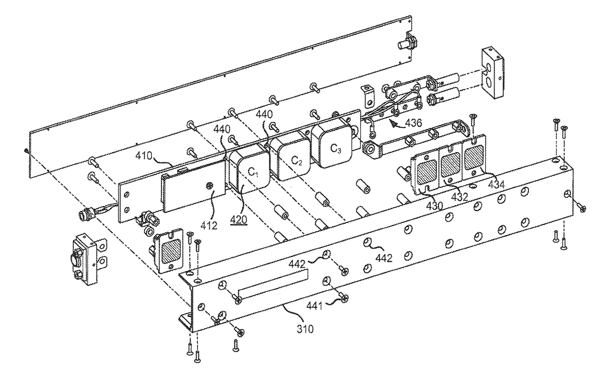
[0010]Some embodiments of the present invention provide a housing with a u-shaped metal channel. The housing provides mechanical and thermal support for a laser diode driver and the u-channel can provide a heat sink for switching elements and capacitor intermediate energy storage. The u-channel may also provide a low loss electrical connection improving rise time and electrical efficiency of the laser diode driver circuit.
[0011]In a particular embodiment, the switching electronics and capacitive energy storage elements are mounted in the metal u-channel. The metallic cases of the capacitors may be directly clamped to the u-channel. Electrically, the u-channel provides a low impedance return path for the large pulse currents flowing in the laser diode loads. The low impedance of the u-channel reduces resistive losses and also minimizes the overall loop inductance of the driver circuit. The loop inductance places voltage stresses on both the electrical switching components and the diode loads. Hence, it is beneficial to reduce the loop inductance. Each time the diode driver produces a pulse of output current; there is a pair of voltage spikes caused by the rapid rate of rise and fall of the current interacting with the inductance. These voltage spikes can damage the laser diodes or the driver electronics. The housing with the u-channel according to embodiments of the present invention provides a low inductance / low resistance path for the voltage spikes so that the laser diodes and / or the diode driver electronics are shielded from these voltage spikes.
[0012]Thermally the u-channel provides a cooling path (i.e., heat sink) for the switching elements, current measuring resistors, and the capacitors. In a tightly packed laser diode array, each driver's u-channel can have a direct electrical connection with the adjoining drivers. The u-channels together provide the negative power supply connection thus reducing the number of cables required to provide DC power to the laser diode array.
[0013]Numerous benefits are achieved by way of the present invention over conventional techniques. For example, embodiments of the present invention provide a small form factor laser diode driver with the higher current density per driver size than conventional designs. Moreover, passive cooling of the laser diode driver components is utilized; removing the active cooling elements (e.g., cooling water lines) typically integrated into high current laser diode drivers. Some embodiments reduce the frontal cross-sectional area, which allows the laser diode driver to be located closer to the laser diode load. This shorter path provides several benefits: 1. A further reduction in the resistive interconnection loses; 2. Reduced parasitic inductance reduces voltage stress on the switching elements and laser diode load; 3. The complexity and length of the DC input power connections are also reduced, resulting in fewer resistive losses; and 4. The design allows for a smaller foot print for the overall laser system, reducing overall system costs. Moreover, in an embodiment, the cooling design provides for better high voltage integrity by separating the coolant from the high voltage elements (e.g., capacitors / switches). The cooling system also allows, in some embodiments, for the elimination of mechanical cooling system (e.g., fans), which are prone to failure. These and other embodiments of the invention along with many of its advantages and features are described in more detail in conjunction with the text below and attached figures.

