
Silicon liner for STI CMP stop in FinFET

a technology of silicon liner and sti cmp stop, which is applied in the direction of basic electric elements, electrical apparatus, and semiconductor devices, can solve the problems that the high-temperature annealing process can damage the underlying fin, and achieve the effect of reducing the height of (removing a portion) and increasing the density of isolation materials

Inactive Publication Date: 2018-05-29
GLOBALFOUNDRIES US INC
View PDF15 Cites 3 Cited by
  • Summary
  • Abstract
  • Description
  • Claims
  • Application Information

AI Technical Summary

Benefits of technology

The methods described in this patent can reduce the material used to isolate certain areas during an etching process, and they also increase the density of that material through a subsequent anneal. Afterward, a second chemical agent is applied to dissolve and remove the hardmask elements used during the etching process. This makes the process easier for patterning the gate insulator and gate conductor on a fin to define the channel region and form the source and drain regions.

Problems solved by technology

However, this can cause problems if chemical mechanical polishing (CMP) processes remove some of the nitride cap.
For example, high-temperature annealing processes can damage the underlying fins if the nitride cap has inadvertently been removed prematurely by overpolishing.

Method used


Image

  • Silicon liner for STI CMP stop in FinFET
  • Silicon liner for STI CMP stop in FinFET
  • Silicon liner for STI CMP stop in FinFET

Examples


Embodiment Construction

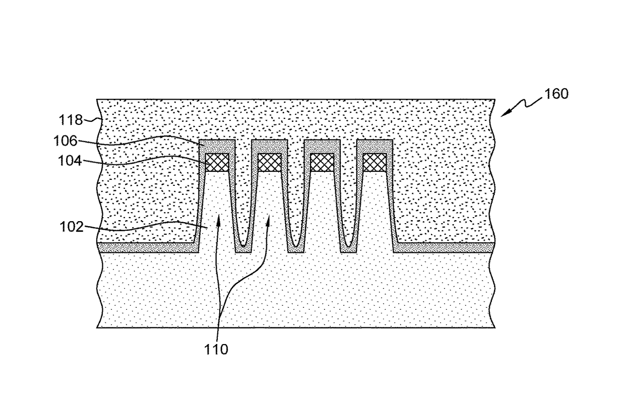
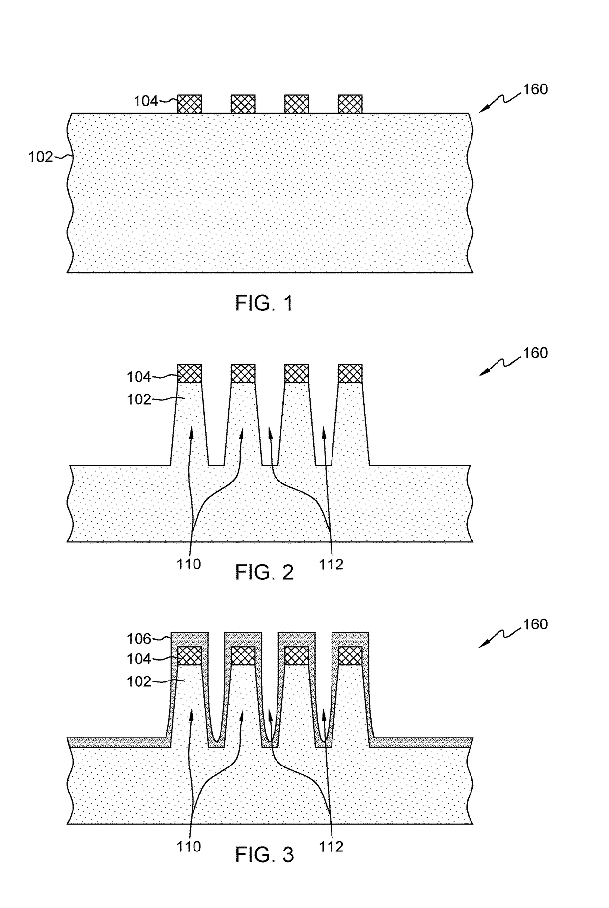
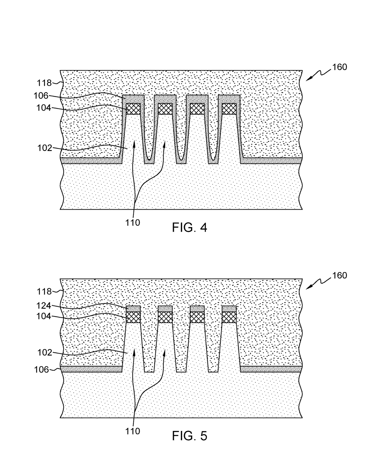
[0014]As mentioned above, if chemical mechanical polishing (CMP) processes remove some of the nitride cap, high-temperature annealing processes can damage the underlying fins; and this problem can be more pronounced at the wafer edge. For example, during a high temperature N2 anneal (that is performed post shallow trench isolation (STI) CMP processing) exposed fins (unbounded) can undergo thermal etching process and be damaged.

[0015]The systems and methods herein address these issues by forming a cap on top of pad nitride (that is thicker than the liner on fin sidewall), using for example, physical vapor deposition (PVD) of silicon, post (after) fin formation. The cap acts as a buffer layer during STI CMP processing to protect the pad nitride hardmask on top of the fin, and this avoids fin exposure during subsequent high temperature anneals. Additionally, this cap improves pad nitride thickness uniformity by protecting the pad nitride from over-polishing, which reduces fin height va...


PUM

PropertyMeasurementUnit
densityaaaaaaaaaa
lengthaaaaaaaaaa
widthaaaaaaaaaa

Abstract

A hardmask is patterned on a first material to leave hardmask elements. The first material is patterned into fins through the hardmask. A layer of silicon is formed on the hardmask elements and the fins in processing that forms the layer of silicon thicker on the hardmask elements relative to the fins. An isolation material is formed on the layer of silicon to leave the isolation material filling spaces between the fins. The isolation material and the layer of silicon are annealed to consume relatively thinner portions of the layer of silicon and leave the layer of silicon on the hardmask elements as silicon elements. A chemical mechanical polishing (CMP) is performed on the isolation material to make the isolation material planar with the silicon elements. A first etching agent removes the silicon elements on the hardmask elements, and a second chemical agent removes the hardmask elements.

Description

BACKGROUNDField of the Invention[0001]The present disclosure relates to manufacturing transistors, and more specifically, to the use of a silicon liner as a shallow trench isolation (STI) chemical mechanical polishing (CMP) stop feature in FinFET processing.Description of Related Art[0002]Integrated circuit devices use transistors for many different functions, and these transistors can take many different forms, from planar transistors, to transistors that use a “fin” style structure. A fin of a fin-type transistor is a thin, long, six-sided rectangle that extends from a substrate, with sides that are longer than they are wide, a top and bottom that have the same length as the sides (but that have a width that is much more narrow), and ends that are as tall from the substrate as the width of the sides, but that are only as wide as the as the top and bottom.[0003]As such fin-type transistors are reduced in size, the nitride cap that is formed on the top of the fin becomes smaller. Ho...

Claims


Application Information

Patent Timeline
Patent Type & Authority Patents(United States)
IPC IPC(8): H01L21/311H01L21/306H01L29/78H01L21/28H01L21/8234
CPCH01L21/823431H01L21/30625H01L29/785H01L21/823481H01L21/28123H01L21/845H01L29/66818
Inventor XU, YIHENGWANG, HAITINGZHAO, WEIABRAMS, TODD B.SHU, JIEHUILIU, JINPINGBEASOR, SCOTT
Owner GLOBALFOUNDRIES US INC
Features
  • Generate Ideas
  • Intellectual Property
  • Life Sciences
  • Materials
  • Tech Scout
  • Unparalleled Data Quality
  • Higher Quality Content
  • 60% Fewer Hallucinations
Learn More