Method of forming trench isolation having polishing step and method of manufacturing semiconductor device

a technology of trench isolation and polishing step, which is applied in the direction of semiconductor/solid-state device manufacturing, electrical equipment, basic electric elements, etc., can solve the problems of difficult polishing and wire disconnection, and achieve the effect of satisfying the flattening shape, easy removal, and convenient removal

Inactive Publication Date: 2003-12-23
SONY CORP
View PDF12 Cites 5 Cited by
  • Summary
  • Abstract
  • Description
  • Claims
  • Application Information

AI Technical Summary

Benefits of technology

Therefore, according to the present invention, it is possible to form a satisfactory flattened shape even in a case where the area ratio of the polishing stopper layer per unit area in the portion to be polished is low.
Further, according to the present invention, the material to be polished on the wide (long) protrusion region, if it remains after polishing, can easily be removed by a removed step using a resist pattern as a mask to conduct flattening, by which It is possible to manufacture a semiconductor device in which flat burying is attained.
Further, according to the present invention, the material to be polished on the wide (long) protrusion region, if it remains after polishing, can be easily removed by the etching back step to achieve flattening. This enables the manufacture a semiconductor device having flat burying of trenches.
Further, according to the present invention, after burying the recesses and depositing the burying material, for example, by CVD, the second polishing stopper layer is formed at least on the recess burying material, for example, on the recess burying material in a portion where the density of the polishing stopper layer is sparse, by which the stopper function can be made nearly uniform over the entire surface of the portion to be polished, the area ratio of the stopper layer can be increased preferably to greater than a predetermined ratio and, thereafter, polishing is performed. Consequently, a uniform and satisfactorily flattened shape can be obtained.
Therefore, according to the present invention, it is possible to form a satisfactorily flattened shape even in a case where the area ratio of the polishing stopper layer per unit area of the polished portion is low. Further, according to the present invention, after burying the recesses, for example, after depositing the burying material by CVD or the like, a second polishing stopper layer is formed at least over the entire surface of the recess burying material, so that the stopper function can be made nearly uniform over the entire surface of the polished portion and the area ratio of the stopper can be increased, preferably, to greater than a predetermined ratio and, subsequently, polishing is performed. Accordingly, a uniform and satisfactorily flattened shape is obtained.
Therefore, according to the present invention, a satisfactorily flattened shape can be formed even in a case where the area ratio of the polishing stopper layer per unit area of the polished portion is low.

Problems solved by technology

This is because unevenness on the underlying substrate, if any, will lead to occurrence of wire disconnection at a step caused by the unevenness (so-called step disconnection).
However, in this method, if a patterning for the block resist is displaced to form a resist out of the recess as shown by reference numeral 31' in FIG. 13(d), no sufficient flatness can be obtained even if a resist coating film 3' is formed, so that the burying material 5 does not become flat as shown in FIG. 13(e) and, as a result, it is difficult to flatten by means of polishing.
That is, the flattening technique by polishing involves a problem that the extent of polishing depends on the underlying pattern and sometimes it results in unevenness.

Method used


Image

  • Method of forming trench isolation having polishing step and method of manufacturing semiconductor device
  • Method of forming trench isolation having polishing step and method of manufacturing semiconductor device
  • Method of forming trench isolation having polishing step and method of manufacturing semiconductor device

Examples


example 1

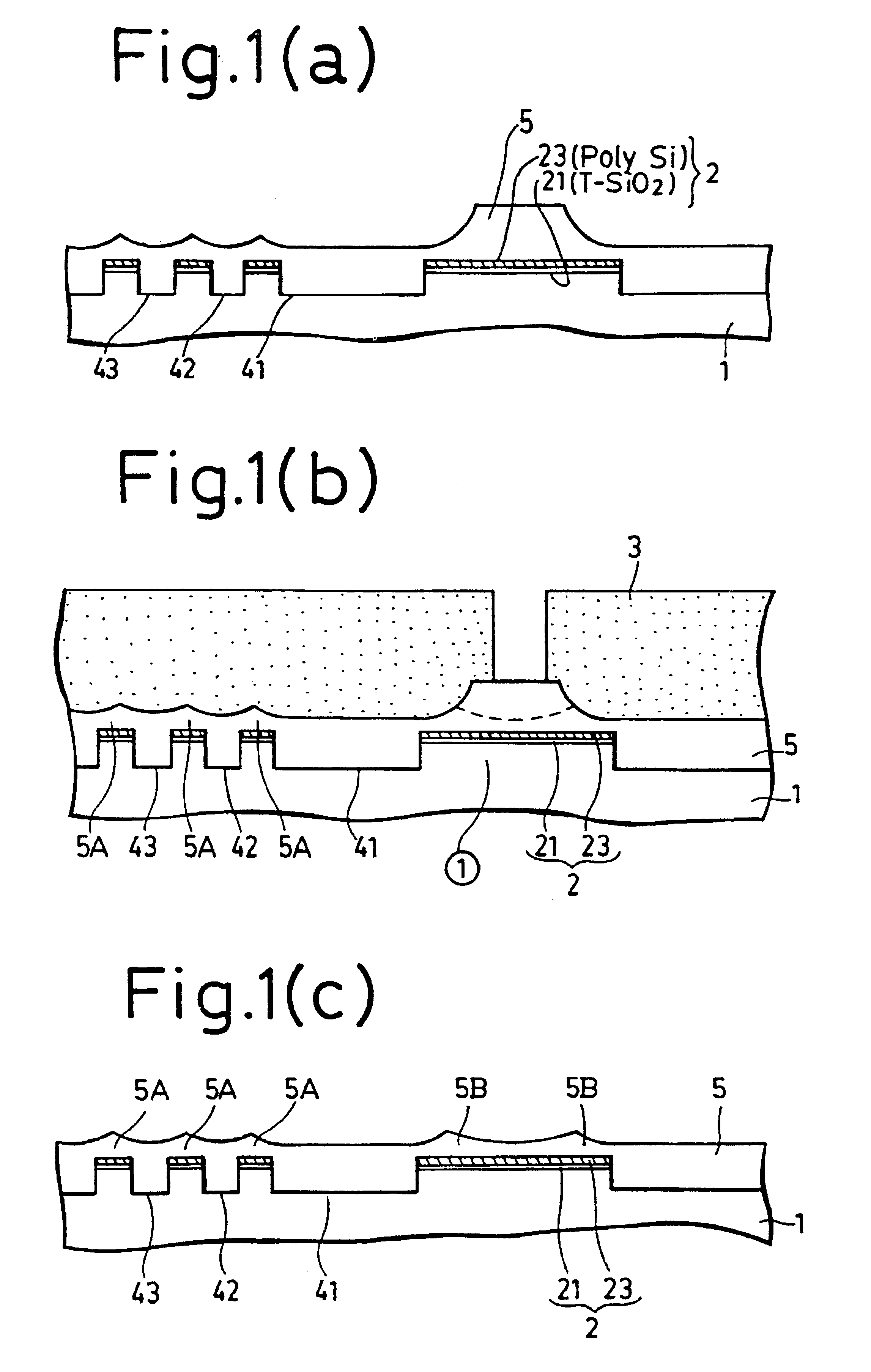
In this example, the present invention is applied to the formation of an integrated a semiconductor device and, in particular, to the formation of trench isolation in the semiconductor device.

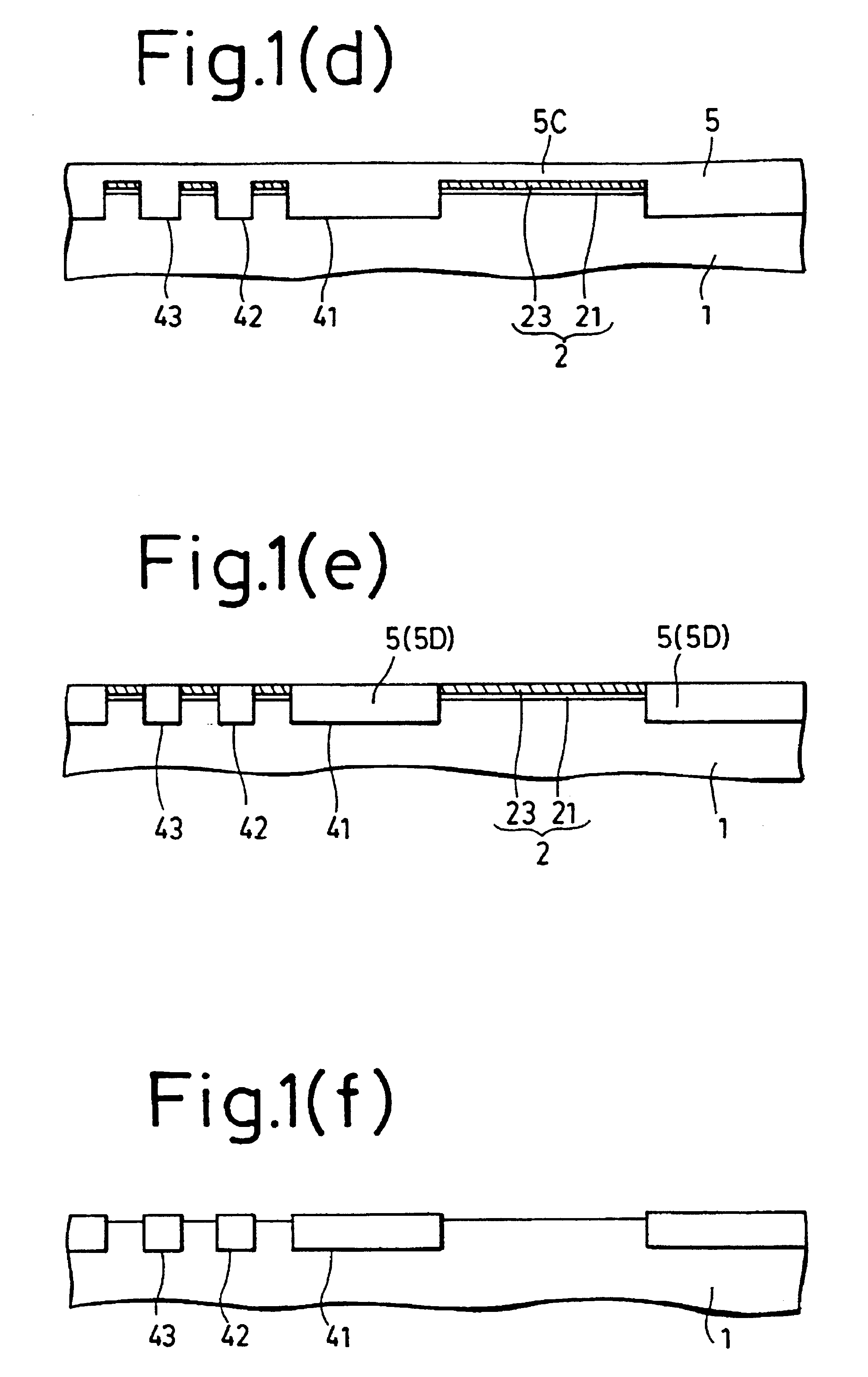
In this example, a structure as shown in FIG. 1(a) is obtained by burying trenches 41-43 by a deposition means that conducts etching and deposition simultaneously (a bias ECR-CVD process is used in this example). Then, an isotropic etching step for isotropically etching the burying material as shown by a broken line in FIG. 1(b) is performed to obtain a structure as shown in FIG. 1(c) before the polishing step. Subsequently, a flat structure as shown in FIG. 1(d) is obtained after the polishing step.

The burying material 5 on a wide protrusion region is etched by the isotropic etching step in FIG. 1(b) into a shape substantially uniform with other portions as shown in FIG. 1(c). Accordingly, a satisfactory flattening is attained by polishing the remaining protruding portions.

More specifically, t...

example 2

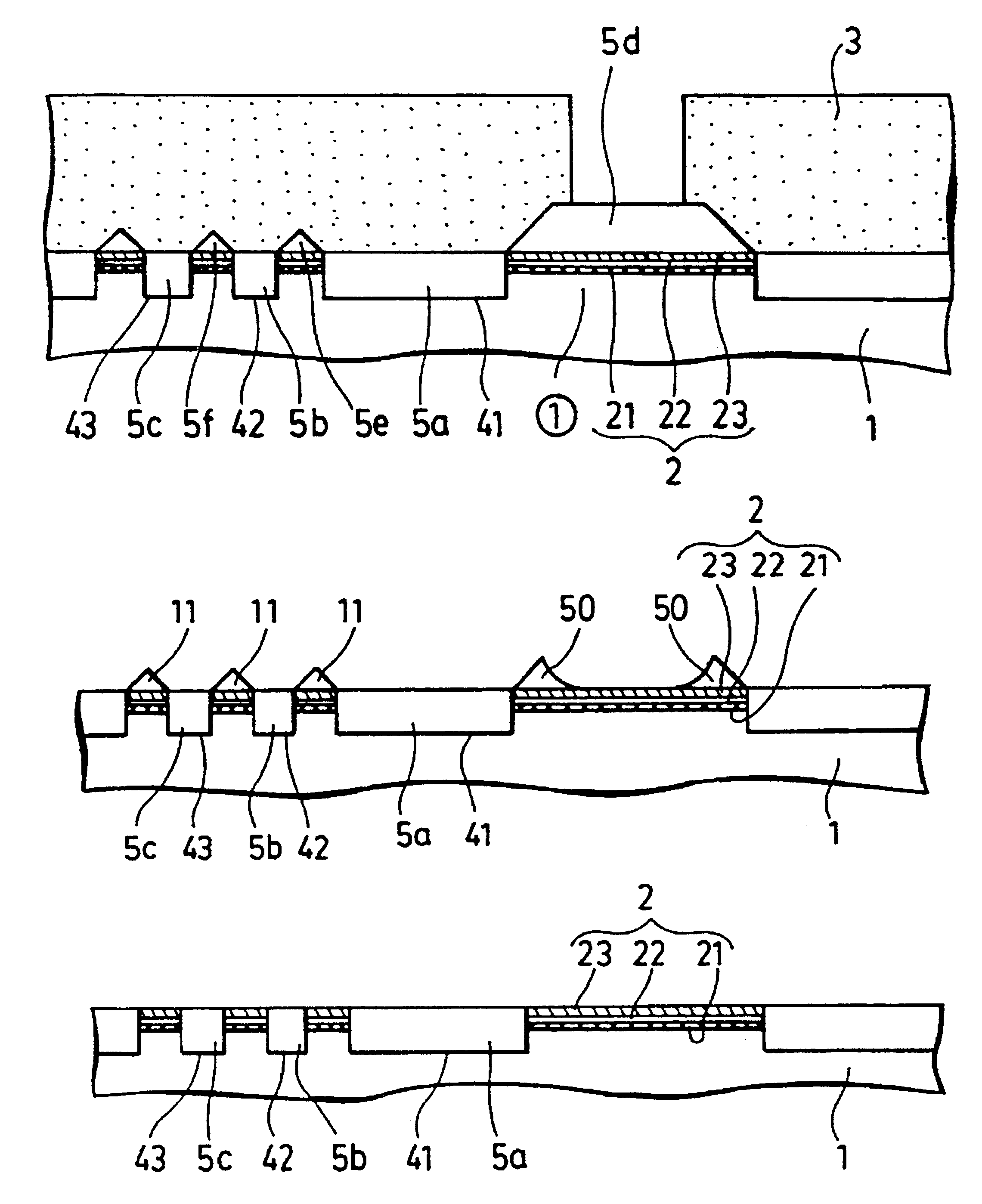
Descriptions will be made to Example 2 which includes formation of trench isolation and manufacture of a semiconductor device.

In Example 1, when the burying material is etched back as far as the upper portion of the trench opening in the state shown in FIG. 2(d), that is, when it is to be etched back by the thickness of the burying material on the protrusion region shown by 5C in FIG. 2(d), since the and point can not be judged, it is difficult to control the etching film thickness as the burying material 5 for the isolation portion shown in FIG. 2(e). Example 2 undertakes to overcome the problem.

In Example 2, since SiO.sub.2 which is the burying material after resist patterning can be etched as far as the surface of the support layer is exposed and the burying material (SiO.sub.2) on the protrusion region can be removed completely by polishing in the next step, etching back which is necessary in Example 1 is no longer required.

In this example, a substrate 1 to be formed with trench...

examples 3 , 4

EXAMPLES 3, 4

The following samples are modified from Examples 1-2 described above. While isotropic etching is applied by wet etching using an etching solution before the polishing of the burying material in Examples 1, 2, isotropic etching was conducted by means of dry etching in these examples.

In the examples, SiO.sub.2 as the burying material 5 was isotropically dry etched under the following conditions, instead of etching by hydrofluoric acid as in Examples 1 and 2:

Etching apparatus used: parallel flat type ether

Pressure: 2300 mtorr (306 Pa)

RF power: 550 W

Gas system used: NF.sub.3 = 300 cc / min He= 200 cc / min

Temperature: 80.degree. C.

Satisfactory isotropic etching could be attained by the conditions described above. The conditions were set in order to increase the power of the conducing reaction using fluoric acid radicals as a main etchant and increase the pressure for reducing the directionality of ions (to shorten the mean free path), thereby attaining isotropic etching.

Other p...


PUM


Abstract

A method of forming trench isolation including a burying step of burying trenches by a deposition means for conducting etching and deposition simultaneously and a polishing step of flattening a burying material by polishing is conducted by disposing an isotropic etching step, a multi-layered etching stopper and a protrusion unifying structure. Polishing can be attained with satisfactory flatness uniformly or with no polishing residue even in a portion to be polished in which the etching stopper layer is distributed unevenly. The method can be applied to manufacture of a semiconductor device or the like.

Description

BACKGROUND OF THE INVENTION1. Field of the InventionThe present invention concerns a method of forming trench isolation having a polishing step and a method of manufacturing a semiconductor device having a polishing step. The present invention can be applied to the formation of trench isolation (trench type inter-device separation) in various kinds of electronic materials, a method of manufacturing various kinds of semiconductor devices braving trench isolation, as well as a method of manufacturing various kinds of semiconductor devices having a recess burying step and a subsequent flattening and polishing step. Further, it can be utilized as a method of manufacturing a semiconductor device having a polishing step including a step of burying recesses defined with a plurality of protrusion patterns (that is, defined between each of protrusion patterns) by a burying material and a step of flattening the burying material formed on the protrusion patterns.2. Description of the Prior Art...

Claims


Application Information

Patent Timeline
Patent Type & Authority Patents(United States)
IPC IPC(8): H01L21/762H01L21/70H01L21/02H01L21/311H01L21/3105H01L21/3065H01L21/304H01L21/76
CPCH01L21/3065H01L21/31053H01L21/31055H01L21/31116H01L21/76229
Inventor GOCHO, TETSUOHAYAKAWA, HIDEAKI
Owner SONY CORP
Why Eureka
Try Eureka