High-frequency IC multi-bus knot tying structure and method

A technology of integrated circuit and wire structure, applied in the direction of circuits, electrical components, electric solid devices, etc., can solve problems affecting circuit characteristics, large electromagnetic interference, and increased metal wire spacing, so as to reduce insertion loss, increase return loss, and improve The effect of high frequency response

Inactive Publication Date: 2007-09-05
VIA TECH INC
View PDF4 Cites 3 Cited by
  • Summary
  • Abstract
  • Description
  • Claims
  • Application Information

AI Technical Summary

Problems solved by technology

[0006] As can be seen from the above, the wire bonding structure in FIG. 1 exposes the following disadvantages: since the pins 160-180 have a considerable distance (usually greater than 0.5mm) between the pins, the chip 110 end to the pin 160 Between -180 terminals, the pitch between metal lines 130-150 increases significantly
[0008] However, although in FIG. 2 the grounding point is set on the exposed part of the chip pad 220 outside the chip 240, the grounding path can be reduced, but the design of the sequential arrangement of the metal lines 270-277 will still generate relatively large electromagnetic interference, which will affect the overall circuit characteristics

Method used


Image

  • High-frequency IC multi-bus knot tying structure and method
  • High-frequency IC multi-bus knot tying structure and method
  • High-frequency IC multi-bus knot tying structure and method

Examples


Embodiment Construction

[0024] In order to have a further cognition and understanding of the features, purposes and functions of the present invention, the detailed description is as follows in conjunction with the accompanying drawings:

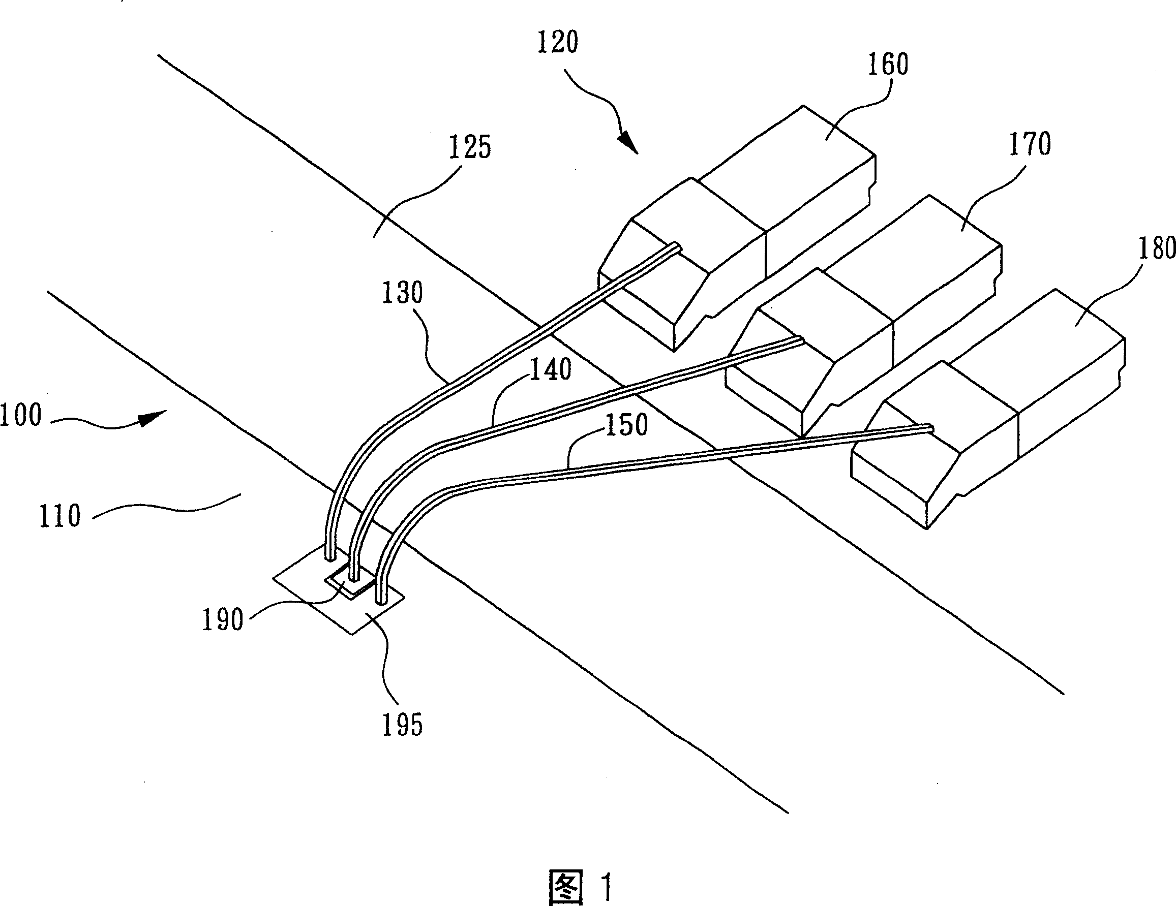
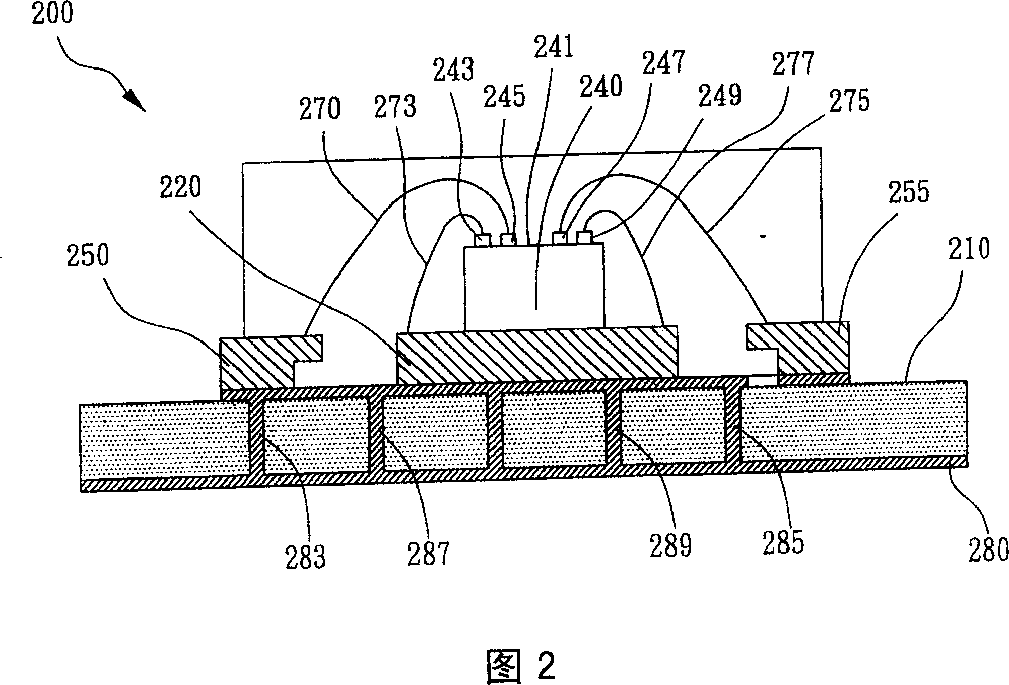
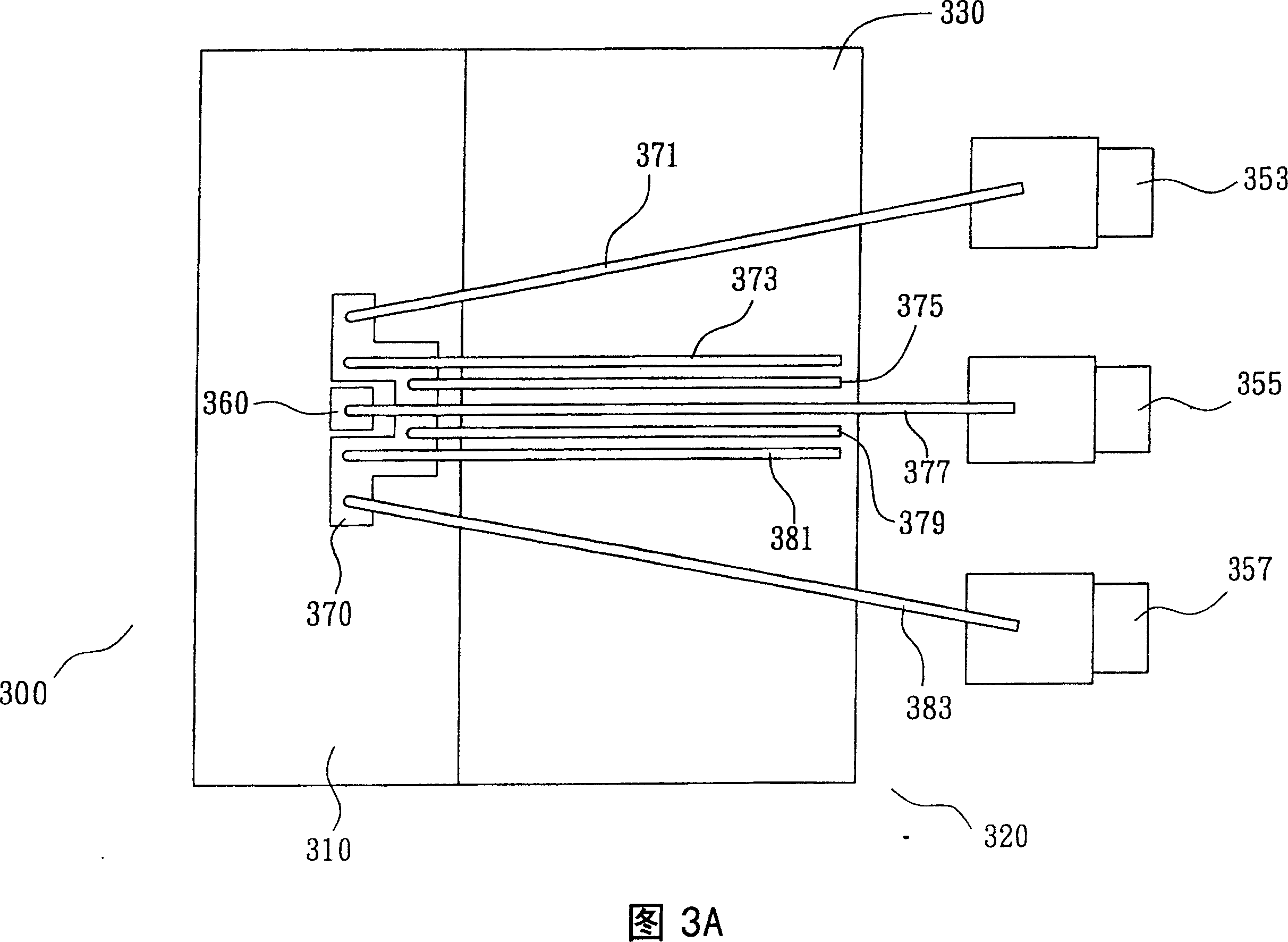
[0025] In view of the defects such as large parasitic capacitance, inductance and relatively large electromagnetic interference that the known wire bonding structure can produce, the present invention considers not only using the coplanar wire pad on the IC chip, but also considering the use of the coplanar wire pad on the coplanar wire pad. The ground wire is bonded on the chip pad under the chip to shorten the distance between the signal ground on the chip. The present invention also specially considers adding grounding metal wires on the coplanar bonding pads to be bonded to the chip pad, and makes a more perfect plan for the arrangement and distribution of the grounding metal wires, so as to effectively reduce the insertion loss between components and increase t...


PUM


Abstract

The presetn invention relates to a multiple column wire wiring structure of high-frequency integrated circuit and its method. Said structure has first electronic component, second electronic component, chip and and several metal wires, in which the first electronic component is fit on the second electronic component by means of chip pad, said structure also includes wiring pads and coplanar wiring pad, and the metal wires are divided into signal wires and ground wires, these metal wires at least can be divided into first column of wires and second column of wires. Said invention also provides the method for implementing said invented multiple column wire wiring structure.

Description

technical field [0001] The invention relates to a high-frequency integrated circuit bonding structure and method, in particular to a high-frequency integrated circuit multi-row wire bonding structure and method that enable the electrical connection between electronic components to have the best electrical characteristics. Background technique [0002] At present, since wire bonding is a relatively cheap and robust circuit connection method, wire bonding is the most commonly used method for circuit connection between IC chips and circuit parts in electronic products. As the operating frequency of electronic products increases day by day, the parasitic inductance and capacitance generated by wire bonding often directly impact the electrical characteristics between the IC chip and the circuit, which cannot be ignored. Therefore, it is worth paying attention to how to reduce these parasitic effects to avoid the decline of electrical characteristics between IC chips and circuits ...

Claims


Application Information

Patent Timeline
Patent Type & Authority Patents(China)
IPC IPC(8): H01L23/50H01L23/52H01L21/60
CPCH01L2224/49112H01L2924/14H01L2924/01005H01L2224/48257H01L24/06H01L2224/06051H01L2924/01082H01L24/03H01L2924/30107H01L2224/49171H01L2224/49175H01L2224/48091H01L24/49H01L24/05H01L2224/48247H01L2224/05552H01L2924/3025H01L2924/01006H01L2924/01033H01L2224/0603H01L2924/3011H01L2224/04042H01L2924/30111H01L2924/181H01L2224/49H01L2924/00014H01L2924/00H01L2924/00012
Inventor 李胜源
Owner VIA TECH INC
Why Eureka
Try Eureka