Method of forming conductive films with micro-wires

a technology of conductive films and micro-wires, which is applied in the direction of photomechanical equipment, instruments, nuclear engineering, etc., can solve the problems of significant reduction of the conductivity of micro-wires, inability to readily form dispersions into conductive compositions, and limited electrical conductivity generated by such conductive compositions, etc., to achieve the desired uniformity, excellent optical properties, and low distortion

Inactive Publication Date: 2015-03-05
EASTMAN KODAK CO
View PDF2 Cites 5 Cited by
  • Summary
  • Abstract
  • Description
  • Claims
  • Application Information

AI Technical Summary

Benefits of technology

[0037]A significant advantage of the present invention is that the transparent conductive electrode formed thereby has very low distortion and desired uniformity (especially when the transparent substrate comprises a flexible material), excellent optical properties (low surface haze of less than 2%, and at least 80% light transmission), and exceptional low electrical resistivity of less than 10 ohms / sq with the conductive micro-wires having an average width of less than 3 μm. The transparent conductive electrode of the present invention can be used to form large touch screen (or panel) displays especially those having flexible transparent polymeric substrates that exhibit an improved high-frequency response.
[0038]The present invention enables the use of conductive compositions distributed within the cured micro-channels having higher amounts of silver. When cured, the conductive compositions exhibit improved conductivity and transparency compared to prior art conductive pastes in which the conductive particles are not properly distributed whereby fine conductive lines and intersections are less likely. Accordingly, the present invention can provide improved micro-wire conductivity and substrate transparency over prior-art devices.
[0039]Thus, it has been demonstrated that the specific sequential features of the method of the present invention, and particularly treating the conductive micro-wires (conductive composition in the photocured micro-channels) with hydrogen chloride, and then polishing the outer surface of the conductive micro-wires in the photocured micro-channels in the presence of water, in that order, effectively results in the formation of micro-wires with enhanced conductivity and the transparency of the resulting conductive article.
[0040]The prior art does not suggest the noted order of method features. If, for example, the hydrogen chloride treatment is carried out after the surface polishing, the micro-wire electrical conductivity is hardly improved. Similarly, if polishing is carried out after the hydrogen chloride treatment but without the presence of water, the removal of residual conductive composition is less effective and the surface is easily scratched, reducing the transparency of the resulting article.

Problems solved by technology

However, the electrical conductivity generated by such conductive compositions is limited after annealing at high temperatures.
However, such dispersions cannot be readily formulated into conductive compositions.
The challenge for using such a method is to completely fill the micro-channels with the conductive composition without retaining residual conductive composition between the micro-channels.
Yet, if the micro-channels are not completely filled with conductive composition, the conductivity of the micro-wires is significantly reduced and if the residual conductive composition is not removed, transparency of substrate and resulting conductive articles are impaired.
Conversely, weak micro-wire adhesion can lead to the micro-wires popping out of the micro-channels and breaking.
It has not been readily apparent how to achieve all of these properties to a satisfactory degree since efforts to improve one feature can diminish another feature.

Method used


Image

  • Method of forming conductive films with micro-wires
  • Method of forming conductive films with micro-wires
  • Method of forming conductive films with micro-wires

Examples


##ventive example 1

Inventive Example 1

Forming a Conductive Film Comprising Micro-Wires

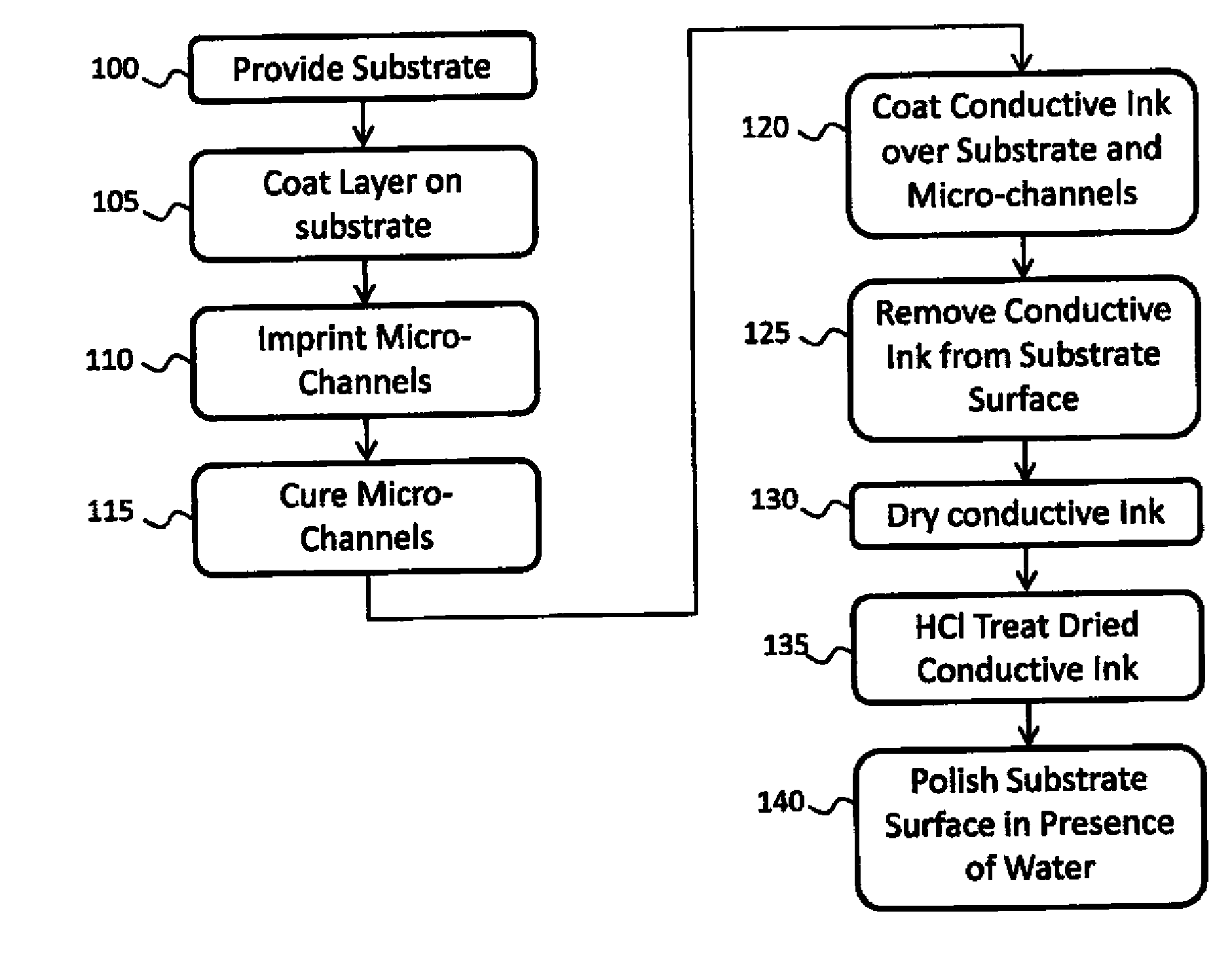
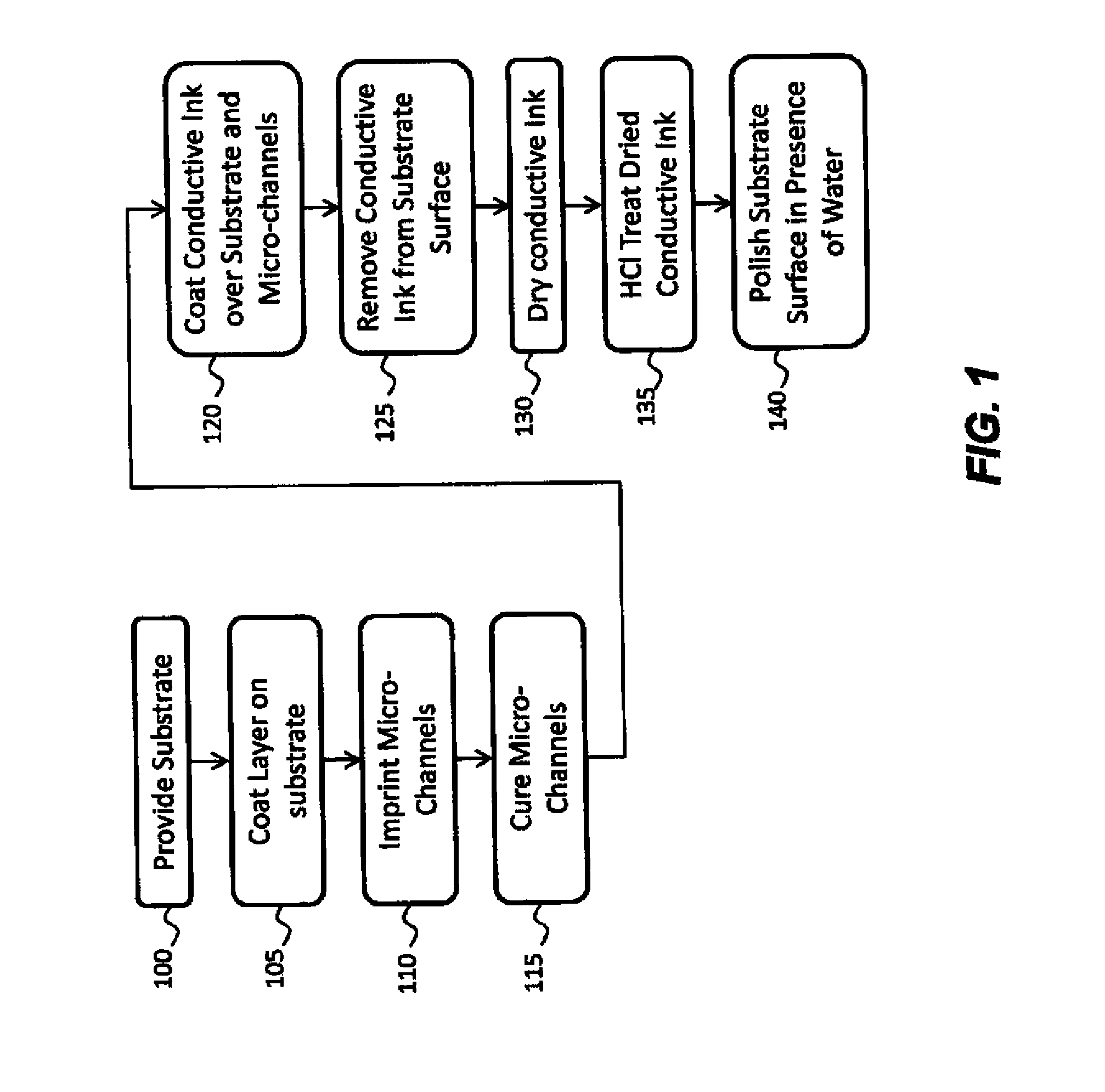
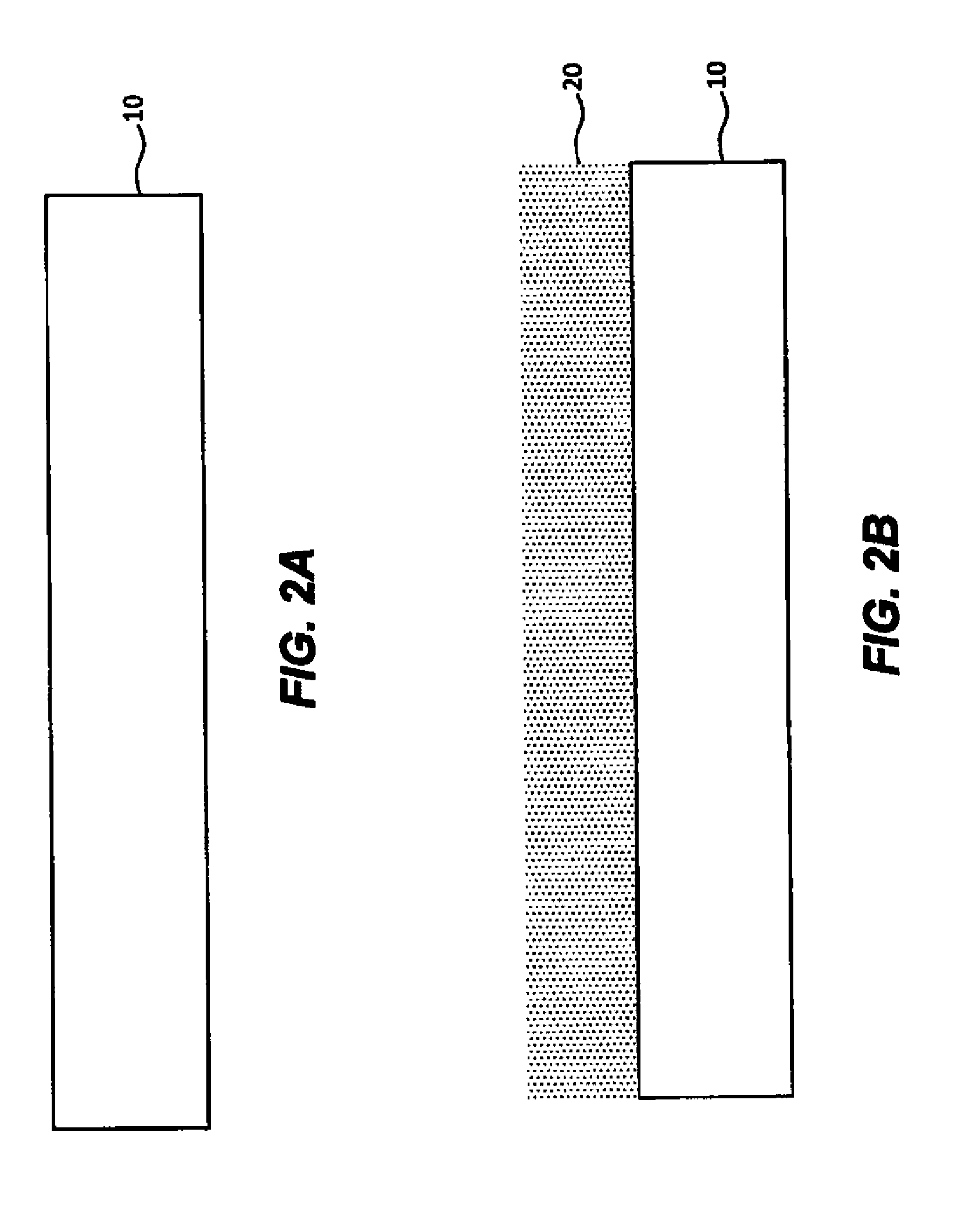
[0127]A poly(ethylene terephthalate) film having a thickness of about 125 μm was surface treated with a poly(vinylidene chloride) containing latex to form an adhesion promotion subbing layer. A coating solution consisting of 34.0 g of Epon resin SU-8, 6.0 g of Coatosil MP-200, 4.8 g of triarylsulfonium hexafluorophosphate salts (mixed), 50% in propylene carbonate, and 55.2 g of methyl ethyl ketone (MEK) was applied as a photocurable composition over the subbing layer and dried to form a photocurable layer having a nominal dry thickness of about 12 μm. The resulting dry film photocurable surface was then laminated with a protective sheet of approximately 25.4 μm thick having one of its surfaces treated with silicone release coating. The protective sheet can be readily separated from the photocurable layer.

[0128]The photocurable layer on the substrate was pressed against a transparent PDMS mold made of Dow Corning Sylg...


PUM

PropertyMeasurementUnit
temperatureaaaaaaaaaa
humidityaaaaaaaaaa
widthaaaaaaaaaa

Abstract

A pattern of conductive micro-wires as in a conductive pattern can be prepared using photo-lithography, or imprint technology. A photocurable composition is cured to form a pattern of photocured micro-channels. A conductive composition comprising metal nano-particles is added to the photocured micro-channels and excess conductive composition outside the photocured micro-channels is removed. The conductive composition in the photocured micro-channels is then dried at a temperature of less than 60° C. The dried conductive composition in the photocured micro-channels is treated with hydrogen chloride vapor to form conductive micro-wires in the photocured micro-channels at a temperature of less than 60° C. The outer surface of the conductive micro-wires is then polished in the presence of water, to form a micro-wire pattern.

Description

CROSS REFERENCE TO RELATED APPLICATIONS[0001]Reference is made to commonly assigned, co-pending U.S. patent application Ser. No. ______ (Attorney Docket K001523) filed concurrently herewith by Wang, Lebens, and Dicillo and entitled “PHOTOCURABLE COMPOSITION, ARTICLE, AND METHOD OF USE,” the disclosure of which is incorporated herein by reference.[0002]Reference is also made to the following commonly assigned and copending patent applications:[0003]U.S. Ser. No. 13 / 746,346 filed Jan. 22, 2013 by Lebens et al.;[0004]U.S. Ser. No. 13 / 746,352 filed Jan. 22, 2013 by Lebens et al.;[0005]U.S. Ser. No. 13 / 757,891 filed Feb. 4, 2013 by Wang et al.;[0006]U.S. Ser. No. 13 / 757,896 filed Feb. 4, 2013 by Wang et al.;[0007]U.S. Ser. No. 13 / 757,899 filed Feb. 4, 2013 by Wang et al.;[0008]U.S. Ser. No. 13 / 757,901 filed Feb. 4, 2013 by Wang et al.;[0009]U.S. Ser. No. 13 / 757,905 filed Feb. 4, 2013 by Wang et al.; and[0010]U.S. Ser. No. 13 / 757,913 filed Feb. 4, 2013 by Wang et al.;[0011]the disclosures...

Claims


Application Information

Patent Timeline
Patent Type & Authority Applications(United States)
IPC IPC(8): H01B13/00H01B1/02H01B13/30
CPCH01B13/0013H01B13/0036H01B1/02H01B13/30H01B13/003G03F7/0002G03F7/038Y10T428/24917
Inventor WANG, YONGCAILEBENS, JOHN ANDREWWRIGHT, MITCHELL LAWRENCE
Owner EASTMAN KODAK CO
Why Eureka
Try Eureka