Capacitance induction system

A capacitive sensing and equivalent capacitance technology, applied in electrical components, electronic switches, electrical digital data processing, etc., can solve the problems of different shapes, sizes, unevenness, and different potentials.

Inactive Publication Date: 2007-10-10
HOLTEK SEMICON
View PDF1 Cites 0 Cited by
  • Summary
  • Abstract
  • Description
  • Claims
  • Application Information

AI Technical Summary

Problems solved by technology

[0004] However, due to factors such as the number of touch buttons, poor design of touch buttons, or uneven distribution of insulating substrate materials, the control circuit cannot uniformly charge the touch buttons of the touch panel, resulting in the Potentials are not the same (uneven), resulting in the potential generated by some touch buttons even lower than the reference value, and it is easy to happen that the finger does not touch the touch buttons, and the control circuit activates the corresponding function.
Therefore, when designing a touch button, the equivalent capacitance of the touch button must be properly adjusted for the above factors, so that the touch button can generate a uniform potential after being charged. However, due to the adjustment of the spiral, comb or The equivalent capacitance of the snake-shaped button, according to the formula: equivalent capacitance C = (dielectric coefficient ε * area A) / line distance D, must be the thickness of the overall line, for example, when increasing the equivalent capacitance, it is not necessary to enlarge the entire button To increase the line width (increase the area) of the graphics, it is necessary to reduce the entire button graphics to reduce the line width (increase the line spacing), but in this way, the buttons will not only have an increased area and different shapes and sizes, which will increase the design difficulty and cost. The problem is that when the wire diameter is reduced, the electric field generated by the equivalent capacitance of the touch key will also decrease, so that the touch key cannot have a good sensing height and sensitivity

Method used


Image

  • Capacitance induction system
  • Capacitance induction system
  • Capacitance induction system

Examples


Embodiment Construction

[0018] A circuit block diagram of a preferred embodiment of the capacitance sensing device of the present invention as shown in Figure 4, the capacitance sensing device 4 of this embodiment is a capacitive touch panel, including an insulating substrate 41 and several capacitance sensing components 42 .

[0019] The insulating substrate 41 is a circuit substrate such as an FR4 board or a flexible board (Membrane), and the capacitive sensing components 42 are used as a touch button, which are formed on the insulating substrate 41 in a matrix arrangement. As shown in FIG. 5 , the structure enlarged view of each capacitive sensing element 42 includes a first electrode 43 and a second electrode 44 .

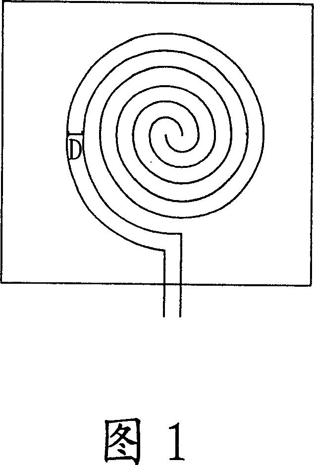
[0020] The first electrode 43 is a circular structure in the present embodiment, has an area (A), and the second electrode 44 is an equidistant distance from the first electrode 43 (distance (D)) around the first electrode 43. The ring on the periphery of the electrode 43 can form an...


PUM


Abstract

The capacitance induction system includes an insulated baseplate and several modules of capacitance induction. The modules of capacitance induction with interval between each other are formed on the insulated baseplate in matrix mode. Each capacitance induction module includes first electrode and second electrode. Second electrode encircle periphery of first electrode with equal interval between them. An equivalent capacitance is formed between first electrode and second electrode. When outer edge of the second electrode is fixed, adjusting distance between inner edge and first electrode changes equivalent capacitance of the capacitance induction module. Thus, when the capacitance induction module is charged, even elctrical level can be generated.

Description

technical field [0001] The invention relates to a capacitive sensing device, in particular to a capacitive sensing device which is easy to adjust the equivalent capacitance of its capacitive sensing component. Background technique [0002] Generally, the sensing interface used in touch panels mainly includes two types: capacitive and resistive. When a touch panel uses a capacitive panel as the sensing interface, it must be mounted on an insulating substrate (such as an FR4 board) or a flexible board ( A plurality of capacitive touch keys are evenly formed on the Membrane as a sensing medium. [0003] The common pattern designs of capacitive touch keys include spiral keys as shown in Figure 1, comb-shaped keys as shown in Figure 2, and snake-shaped keys as shown in Figure 3. The linear, comb-shaped or snake-shaped structure forms an equivalent capacitance on the key. In this way, when a control circuit sends a pulse signal to charge the touch buttons formed on the touch pan...

Claims


Application Information

Patent Timeline
IPC IPC(8): H03K17/955G06F3/023
Inventor 林怡诚
Owner HOLTEK SEMICON
Why Eureka
Try Eureka