A varactor diode structure used in a flash memory circuit and a manufacturing method thereof
A varactor diode and flash memory technology, which is applied in the direction of circuits, semiconductor/solid-state device manufacturing, electrical components, etc., can solve the problem of chip area reduction and achieve the effect of expanding and improving capacitance
- Summary
- Abstract
- Description
- Claims
- Application Information
AI Technical Summary
Problems solved by technology
Method used
Image
Examples
Embodiment 1
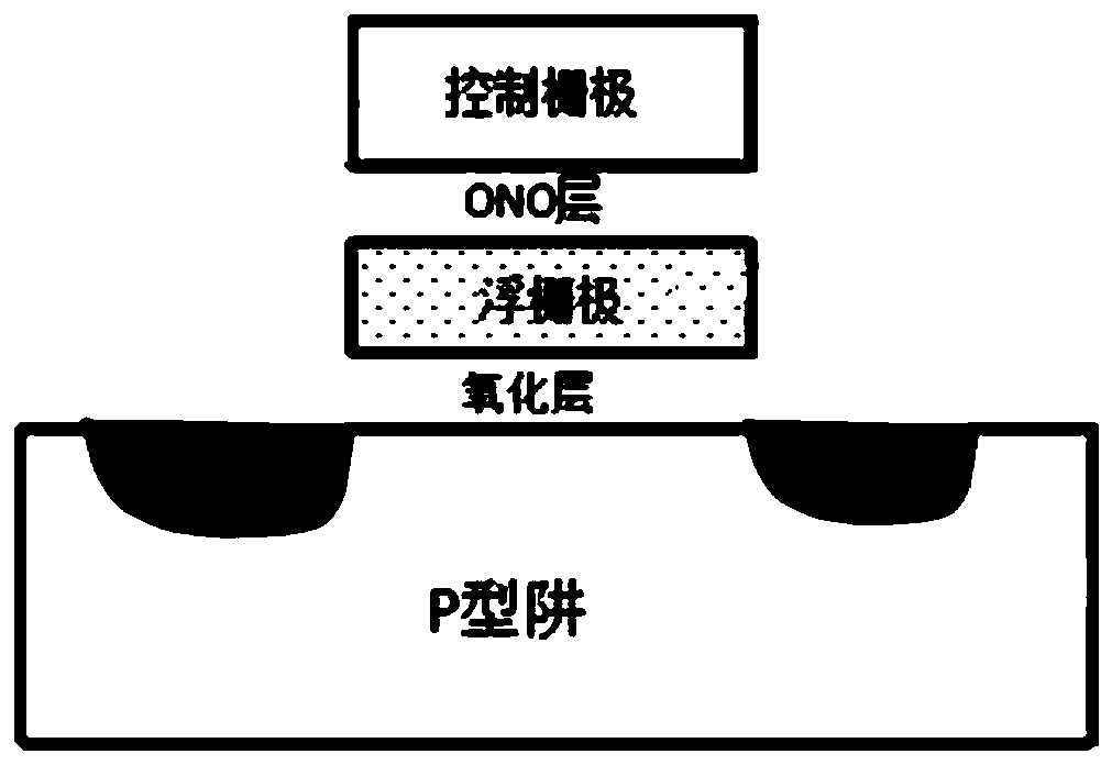
[0047] see Figure 4 , Figure 4 It is a schematic diagram of a preferred embodiment of the varactor diode structure used in the flash memory circuit of the present invention. The varactor diode includes a substrate 1, a first insulating layer 2 formed on the substrate 1, a floating gate 3 formed on the first insulating layer 2, and a control gate opposite to the floating gate 3 4, and the second insulating layer 5 formed between the floating gate 3 and the control gate 4, the first insulating layer 2 is also called a tunnel oxide layer, and a source and a drain are formed on the substrate 1.
[0048] In this embodiment, preferably, the material of the first insulating layer 2 may be silicon dioxide, and the second insulating layer 5 may be a silicon oxide / silicon nitride / silicon oxide (ONO) structure.
[0049] The floating gate 3 is separately drawn out as a pole plate, image 3 It illustrates a lead-out method provided by the embodiment of the present invention, that is, ...
Embodiment 2
[0054] see Figure 5 , Figure 5 It is a schematic diagram of another preferred embodiment of the varactor diode structure used in the flash memory circuit of the present invention.
[0055] The varactor diode structure used in the flash memory circuit provided by this embodiment can include all the structural elements in the flash memory transistor structure of the first embodiment, the difference is that the floating gate 3 of the varactor diode structure in the first embodiment can be viewed from its side Leading out, in the embodiment of the present invention, the leading out line of the floating gate 3 needs to pass through the second insulating layer 5 and the control gate 4 . Its formation process includes:
[0056] On the control grid 4 and the second insulating layer 5, vertically connected through holes are respectively formed, and a contact hole is formed in the through hole through the insulating layer to connect with the floating gate 3, thereby leading out the ...
PUM
 Abstract
Description
Claims
Application Information


