Embedded capacitor structure and manufacturing method thereof

A capacitor structure and manufacturing method technology, applied in the field of capacitors, can solve problems such as large parasitic capacitors, achieve the effects of reducing area, realizing diversity, and ensuring verticality

Pending Publication Date: 2022-02-25
泉州市三安集成电路有限公司
View PDF0 Cites 0 Cited by
  • Summary
  • Abstract
  • Description
  • Claims
  • Application Information

AI Technical Summary

Problems solved by technology

In addition, when a large-area MIM capacitor is used, it will not only occupy a large area on the integrated circuit, but also generate relatively large parasitic capacitance

Method used


Image

  • Embedded capacitor structure and manufacturing method thereof
  • Embedded capacitor structure and manufacturing method thereof
  • Embedded capacitor structure and manufacturing method thereof

Examples


Embodiment 1

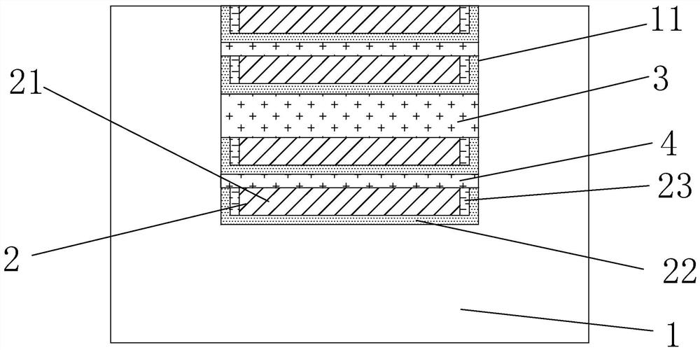
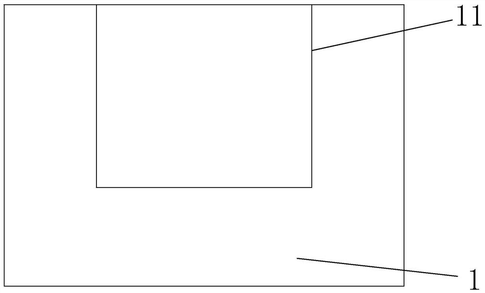
[0036] refer to figure 1 , the embedded capacitive structure proposed by the embodiment of the present application includes a substrate and at least one set of capacitive structures 2 . Where there is a trench 11 with a certain depth on the substrate 1, and a third dielectric layer 3 may be arranged between two adjacent groups of capacitive structures 2, at least two groups of capacitive structures 2 and the third dielectric layer 3 in the middle are laminated and arranged in the trench 11 constitutes an embedded capacitor. Wherein, the thickness of the substrate 1 is 625-665 μm, and the material of the substrate 1 includes Si or GaAs. The depth of the trench 11 is 10 μm˜100 μm, and the sidewall of the trench 11 has a certain verticality in the substrate 1 . Specifically, the included angle between the sidewall of the ditch 11 and the bottom of the ditch 11 is 88°-92°. From the bottom of the trench 11 along the depth direction of the trench 11, multiple layers of the capaci...

Embodiment 2

[0050] refer to figure 1 , another embedded capacitor structure, which differs from the first embodiment in that the adhesive layer 22 is made of Si, and the electrode layer is manufactured using a self-aligned silicide (Salicide) process in step 4. Therefore, in the case where the adhesive layer 22 is Si, the electrode layer is deposited on the surface of the Si layer, and the electrode layer is in contact with the surface of the Si layer. Then heat treatment is performed to form a silicide electrode layer on the surface of the contact electrode layer and the Si layer. In step 5, the first dielectric layer and the Si layer on the sidewall of the ditch above the silicided electrode layer are removed, wherein the electrode layer can be selected from one of the metals Ti, Co, and Ni.

Embodiment 3

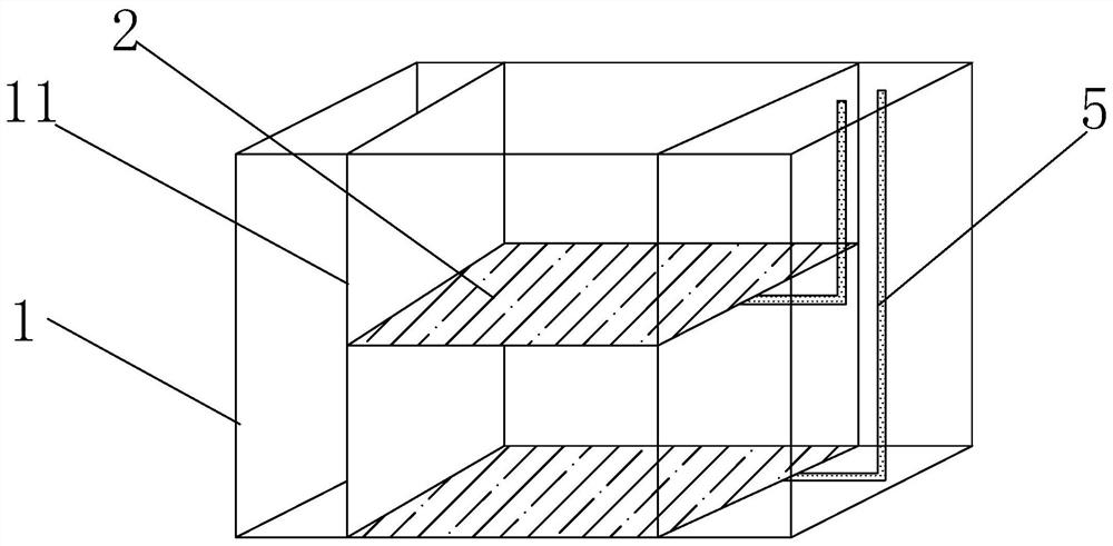
[0052] refer to Figure 4 , another embedded capacitor structure, which is different from Embodiment 1 in that an air layer 5 is between two adjacent capacitor structures. Specifically, in step 6, a sacrificial material is filled between two adjacent capacitor structures, and the third dielectric layer 3 is set as a sacrificial layer. In the manufacturing method, step 8 further includes: forming an air layer 5 between two sets of adjacently spaced capacitor structures by opening holes and removing the sacrificial layer after the fabrication of the last group of capacitor structures is completed. Sacrificial material can choose SOG.


PUM

PropertyMeasurementUnit
heightaaaaaaaaaa
thicknessaaaaaaaaaa
thicknessaaaaaaaaaa

Abstract

The invention discloses an embedded capacitor structure and a manufacturing method thereof, the capacitor structure comprises a substrate with a trench with a certain depth, the bottom of the trench is sequentially provided with multiple layers of electrode structures which are arranged at intervals along the depth direction of the trench, and each electrode structure comprises an electrode layer, and a bonding layer and a first dielectric layer which are arranged around the electrode layer; the first dielectric layer and the bonding layer sequentially wrap the side wall of each electrode layer, the electrode structures are attached to the side wall of the trench through the bonding layers, each bonding layer further wraps the bottom faces of the electrode layer and the first dielectric layer, and a second dielectric layer is arranged between every two adjacent spaced electrode structures. And two adjacent and spaced electrode structures and the second dielectric layer between the two adjacent and spaced electrode structures form a group of capacitor structures. The DRIE and depth end point detection technology is adopted to form the trench with the vertical side wall, the thickness, the area and the shape of the capacitor structure can be adjusted according to requirements, variable control over the capacitance value is achieved, and finally the purpose of optimizing the efficiency is achieved.

Description

technical field [0001] The invention relates to the field of capacitors, in particular to an embedded capacitor structure and a manufacturing method thereof. Background technique [0002] With the advancement of science and technology, 5G wireless communication, GPS and other technologies have emerged, and the technical requirements for high-performance radio frequency circuits and passive devices (IPD) have gradually increased. Capacitance, as a commonly used electronic device in the fields of high-performance radio frequency circuits and passive devices, plays an important role in the manufacture of semiconductor circuits. [0003] Capacitor is also a key part in the manufacturing process of integrated filter (filter). The capacitance value of the capacitor is the main factor to determine the target frequency of the filter, and the capacitance value is determined by the thickness and area of ​​the dielectric layer. The current capacitor is based on the MIM (metal-insulato...

Claims


Application Information

Patent Timeline
Patent Type & Authority Applications(China)
IPC IPC(8): H01L49/02
CPCH01L28/40H01L28/60
Inventor 朱庆芳
Owner 泉州市三安集成电路有限公司
Why Eureka
Try Eureka