Capacitor and layout method thereof

A layout method and capacitor technology, which is applied in capacitors, electric solid devices, circuits, etc., can solve problems such as low capacitance matching accuracy, unsuitable design requirements, and inconsistent capacitance values, and achieve the effect of improving capacitance matching accuracy

Inactive Publication Date: 2016-09-07
WUHAN SYNTEK CO LTD
View PDF7 Cites 0 Cited by
  • Summary
  • Abstract
  • Description
  • Claims
  • Application Information

AI Technical Summary

Problems solved by technology

Considering that the resistance and capacitance of the wires connecting the device to the circuit in practical applications will lead to low capacitance matching accuracy and even cause system mismatch, layout designers minimize the wire capacitance by increasing the size of a single capacitor, but This method is not suitable for all design requirements. The reasons include: the increase of the capacitor size will affect the area of ​​the integrated circuit, the increase of the capacitor size makes the capacitance value of the capacitor not meet the design requirements, or the design requirements of high-precision capacitor matching cannot be met.
[0005] All in all, in the prior art, there is a method of reducing the difference rate of the wire capacitance by changing the size of a single capacitor, thereby improving the capacitance matching accuracy, which limits the technical problem of integrated circuit design

Method used


Image

  • Capacitor and layout method thereof
  • Capacitor and layout method thereof
  • Capacitor and layout method thereof

Examples


Embodiment 1

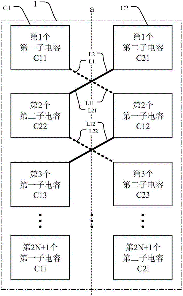
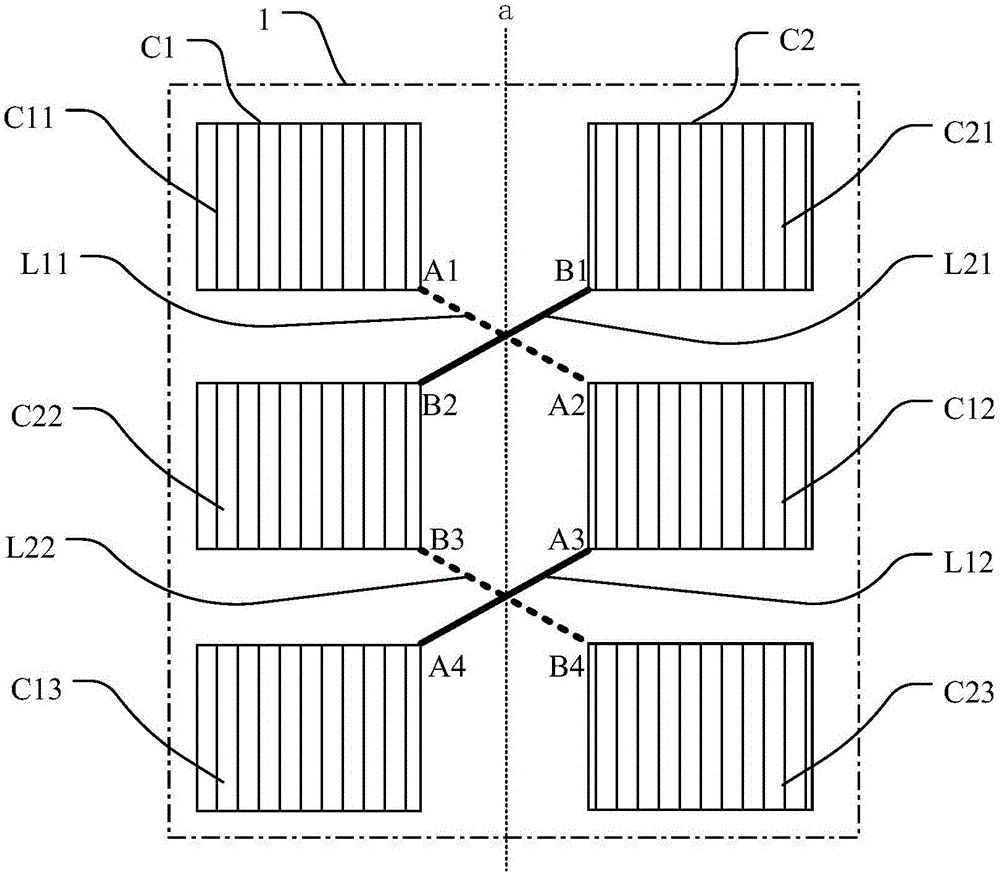
[0034] Please refer to figure 1 , the embodiment of the present invention provides a capacitor 1, including:

[0035] Symmetrically arranged first capacitor C1 and second capacitor C2;

[0036] The first capacitor C1 includes the first group of metal wiring L1 and 2N+1 first sub-capacitors (C11~C1i), and the second capacitor C2 includes the second group of metal wiring L2 and 2N+1 second sub-capacitors (C21 ~C2i); wherein, N is a positive integer, i is equal to 2N+1, 2N+1 first sub-capacitors (C11~C1i) are sequentially connected through the first group of metal connection lines L1, and 2N+1 second sub-capacitors ( C21~C2i) are sequentially connected through the second group of metal connection lines L2; ​​2N+1 first sub-capacitors (C11~C1i) and 2N+1 second sub-capacitors (C21~C2i) The symmetry axis a of the capacitor C2 is arranged crosswise;

[0037] The difference rate between the capacitance sum of 2N+1 first sub-capacitors (C11~C1i) and the sum of capacitance values ​​o...

Embodiment 2

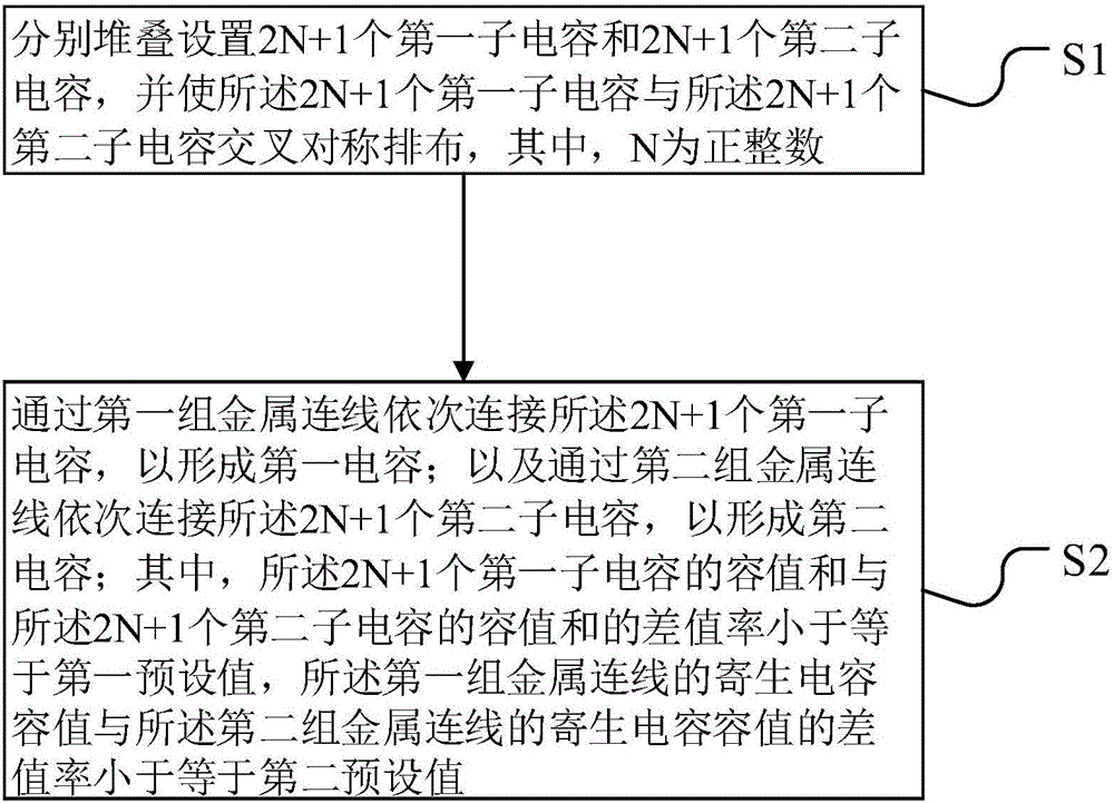
[0051] Based on the same inventive concept, please refer to image 3 , the present application also provides a capacitor layout method, comprising the following steps:

[0052] S1, respectively stacking 2N+1 first sub-capacitors and 2N+1 second sub-capacitors, and making the 2N+1 first sub-capacitors and the 2N+1 second sub-capacitors cross-symmetrically arranged , where N is a positive integer;

[0053] S2. Connect the 2N+1 first sub-capacitors sequentially through the first group of metal wires to form a first capacitor; and sequentially connect the 2N+1 second sub-capacitors through the second group of metal wires to form forming a second capacitor; wherein, the difference rate between the capacitance sum of the 2N+1 first sub-capacitors and the capacitance sum of the 2N+1 second sub-capacitors is less than or equal to a first preset value, and the A difference rate between the parasitic capacitance of the first group of metal connections and the parasitic capacitance of ...


PUM


Abstract

The invention discloses a capacitor and a layout method thereof, and aims at solving the problem that the integrated circuit design is limited by an existing method of reducing the difference ratio of a lead capacitance by changing the sizes of single capacitors to improve the capacitance matching precision. The capacitor comprises a first capacitor (C1) and a second capacitor (C2), which are in cross symmetric arrangement along an axis (a), wherein the first capacitor (C1) comprises 2N+1 first sub-capacitors (C11-C1i) which are sequentially connected through a first group of metal lines (L1); the second capacitor (C2) comprises 2N+1 second sub-capacitors (C21-C2i) which are sequentially connected through a second group of metal lines (L2); N is a positive integer; i is 2N+1; the difference ratio of the capacitance sum of the sub-capacitors (C11-C1i) and the sub-capacitors (C21-C2i) is not greater than a first preset value; and the difference ratio of the parasitic capacitances of the first group of metal lines (L1) and the second group of metal lines (L2) is not greater than a second preset value. The effect of improving the capacitance matching precision under the premise of not changing the sizes of the single capacitors is achieved.

Description

technical field [0001] The invention relates to the technical field of integrated circuit layout design, in particular to a capacitor and a layout method thereof. Background technique [0002] In the manufacturing process of integrated circuits, metals, dielectrics and other materials are fabricated on the surface of silicon wafers by various methods such as physical vapor deposition and chemical vapor deposition to form electronic components and metal interconnections between components Each metal structure layer is connected with a plurality of metal-filled through holes, which makes the circuit have high complexity and circuit density. An important indicator of integrated circuit performance is path delay, that is, the time required from an input to an output; the path delay of an integrated circuit includes device delay and interconnect delay between devices. With the reduction of process nodes and the increase of the number of devices, the delay of the interconnect lin...

Claims


Application Information

Patent Timeline
Patent Type & Authority Applications(China)
IPC IPC(8): H01L23/64H01L27/02
CPCH01L23/642H01L27/0207H01L28/40
Inventor 张科峰刘薇谭珍
Owner WUHAN SYNTEK CO LTD
Why Eureka
Try Eureka