Method for eliminating static electricity of metal conducting layer to complete etching

A metal conductive layer and etching technology, which is applied in the manufacturing of circuits, electrical components, semiconductor/solid-state devices, etc., can solve the problems of incomplete etching and wafer process yield decline, and achieve the effect of completely improving etching

Inactive Publication Date: 2007-10-24
SEMICON MFG INT (SHANGHAI) CORP +1
View PDF0 Cites 0 Cited by
  • Summary
  • Abstract
  • Description
  • Claims
  • Application Information

AI Technical Summary

Problems solved by technology

For example (as shown in FIG. 1 ), it is known that a metal conductive layer 1a is usually located above an oxide layer 5a; a nitride layer 2a is deposited on the metal conductive layer 1a by plasma vapor deposition, and the metal Conductive layer 1a in the process of plasma vapor deposition, or through dry air friction, there will be a positive charge static electricity 11a accumulated in the situation of the metal conductive layer 1a; the positive charge static electricity 11a on the metal conductive layer 1a Forming an energy barrier makes it difficult for some positively charged etching ions 4a to enter a round hole or the bottom of the groove 31a next to a fluorosilicate glass 3a (especially when the round hole or the groove is smaller), so the etching ions 4a is difficult to perform etching reaction with the nitride layer 3a, thus causing incomplete etching, which will cause a decrease in yield in the wafer manufacturing process

Method used


Image

  • Method for eliminating static electricity of metal conducting layer to complete etching
  • Method for eliminating static electricity of metal conducting layer to complete etching
  • Method for eliminating static electricity of metal conducting layer to complete etching

Examples


Embodiment Construction

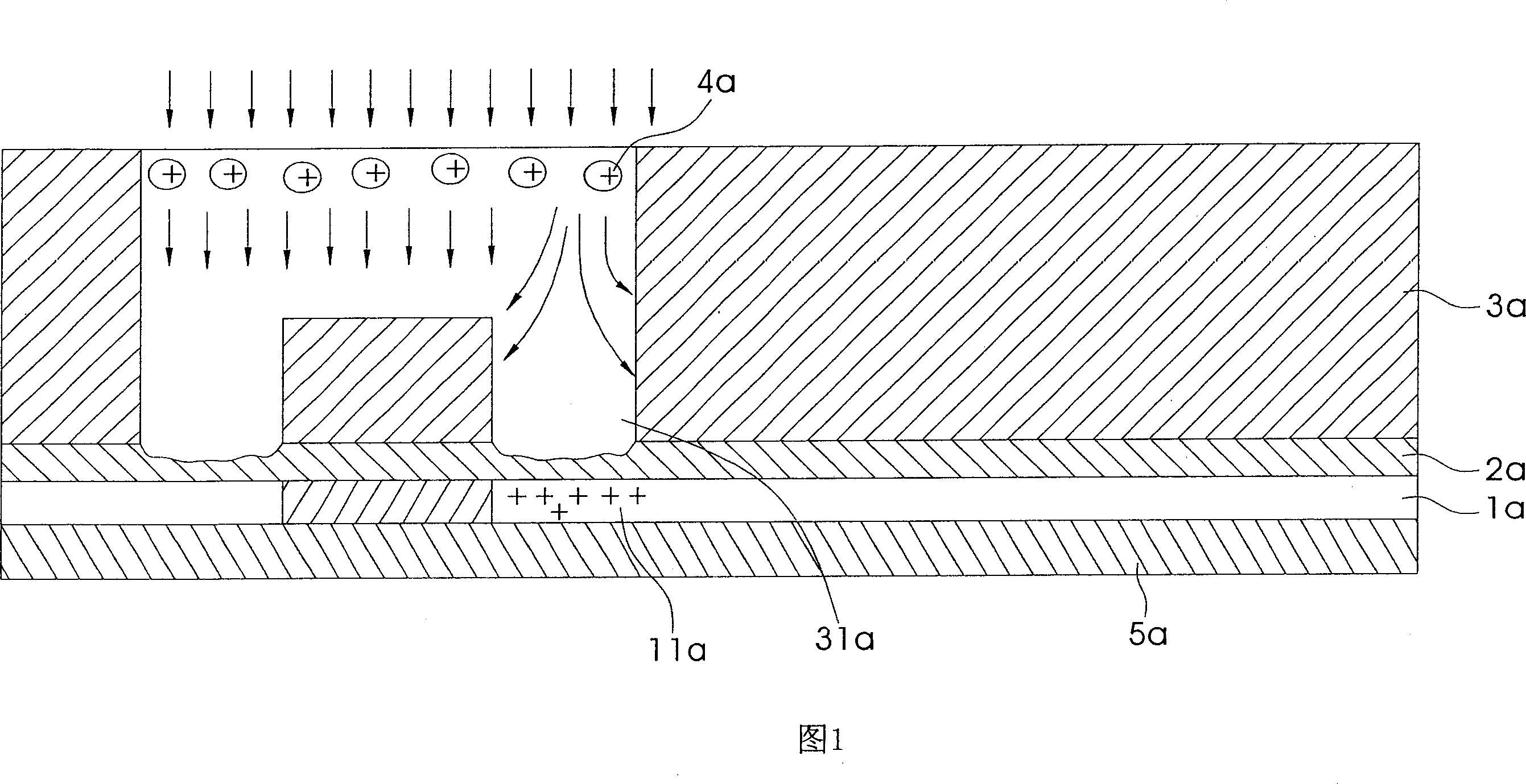
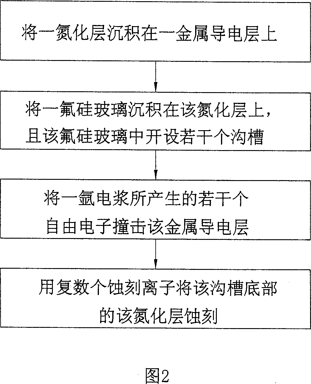
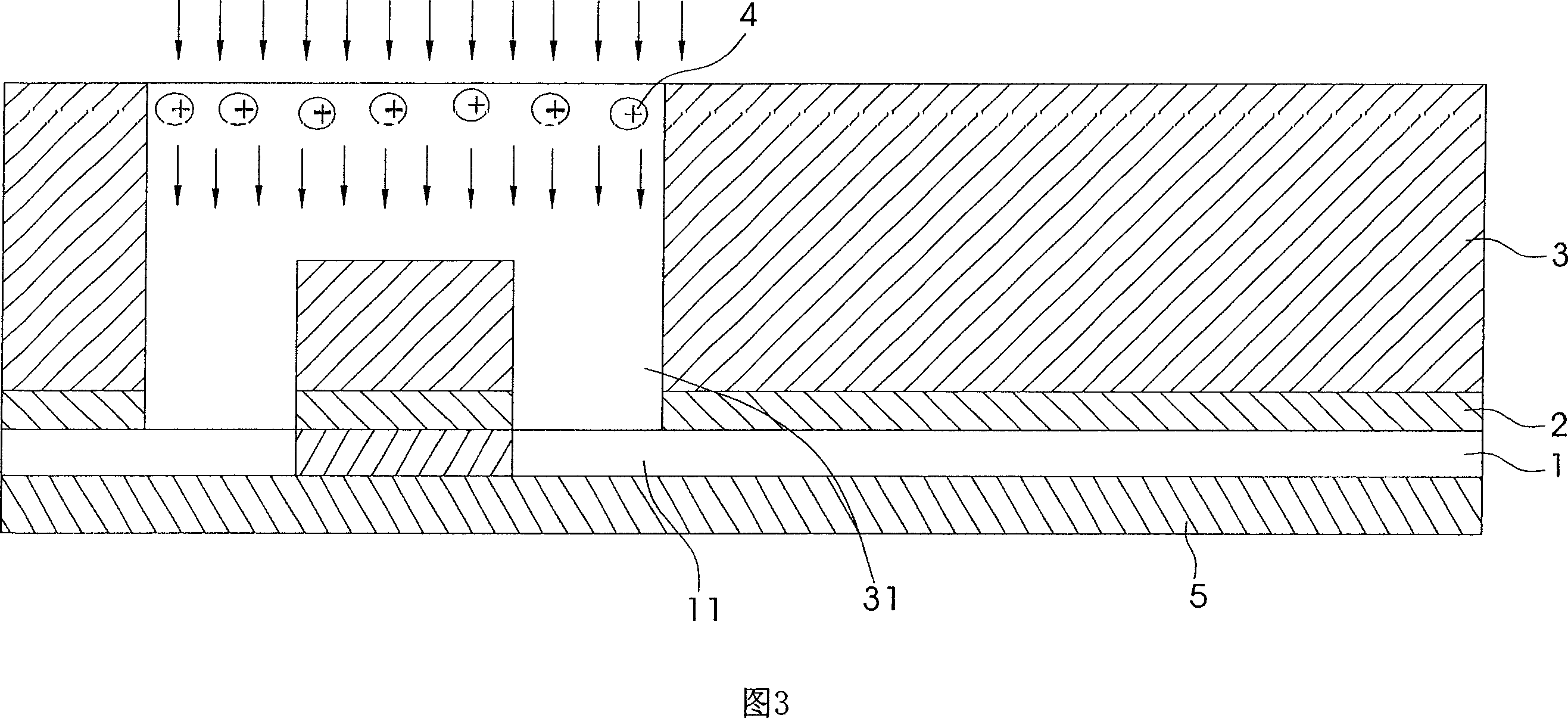
[0025] The present invention eliminates the static electricity of metal conduction layer and makes the method for etching completely, and its step (as shown in Figure 2) comprises: a. a metal conduction layer 1 (as copper layer) is deposited on an oxide layer 5, then a nitrogen An oxide layer 2 (such as a silicon nitride layer) is deposited on the metal conductive layer 1;

[0026] b. A fluorosilicate glass 3 is deposited on the nitrided layer 2, and several round holes or grooves 31 are opened on the fluorosilicate glass 3, and the bottom of the round holes or grooves 31 is the nitrided layer. Layer 2;

[0027] c. A number of free electrons generated by a high-pressure low-density plasma are bumped into the metal conductive layer 1 to neutralize a positively charged static electricity 11 on the metal conductive layer 1, so that the metal conductive layer 1 has an electric charge be neutral or have a number of negatively charged free electrons; and

[0028] d. Etching the ni...


PUM


Abstract

This invention relates to a method to remove metal conductive layer static complete etching, which comprises the following steps: a, depositing a metal conductive layer on the on nitrogen layer; b, depositing a fluorin and silicon glass on the nitrogen layer with several round holes and grooves opened; c, using the electric plasm with high gas pressure and low density generated free electrons impacting the metal conductive layer; d, etching the nitrogen layer on the round holes and groove bottom by several etching ions.

Description

technical field [0001] In the manufacturing process of the wafer, the positive charge and static electricity will accumulate on the metal conductive layer to form a barrier of potential energy. When the hole or the groove is smaller, the nitride layer on the metal wire layer will be difficult to etch completely. The present invention The method of eliminating the static electricity of the metal conductive layer to complete the etching can eliminate the positive charge static electricity accumulated on the metal conductive layer, so that the nitride layer at the bottom of the round hole or the trench can be completely etched. Background technique [0002] It is known that in the plasma etching process of semiconductors, some etching incompleteness occurs; the incomplete etching is caused by electrostatic accumulation of positive charges on the metal conductive layer. For example (as shown in FIG. 1 ), it is known that a metal conductive layer 1a is usually located above an ox...

Claims


Application Information

Patent Timeline
Patent Type & Authority Patents(China)
IPC IPC(8): H01L21/321H01L21/3213
Inventor 吴汉明宋伟基邢国强古其发
Owner SEMICON MFG INT (SHANGHAI) CORP
Why Eureka
Try Eureka