Solid image sensor and image fetching method

A solid-state image and sensor technology, applied in image communication, electrical solid-state devices, semiconductor devices, etc., can solve problems such as distortion, offset, and detection time lag

Inactive Publication Date: 2007-11-14
FUJITSU MICROELECTRONICS LTD
View PDF8 Cites 2 Cited by
  • Summary
  • Abstract
  • Description
  • Claims
  • Application Information

AI Technical Summary

Problems solved by technology

Doing this sequentially for other rows often creates "skew" and "distortion" due to detection time lag between rows

Method used


Image

  • Solid image sensor and image fetching method
  • Solid image sensor and image fetching method
  • Solid image sensor and image fetching method

Examples


no. 1 example

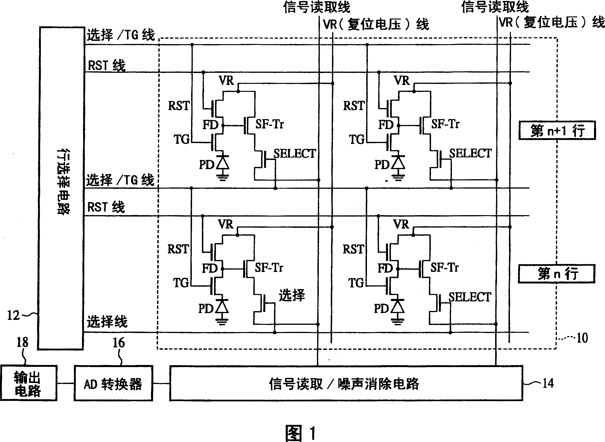
[0055] A solid-state image sensor according to a first embodiment of the present invention will be described below with reference to FIGS. 1-8.

[0056] FIG. 1 is a circuit diagram of a solid-state image sensor according to this example. 2-5 are plan views showing the structure of a solid-state image sensor according to a first embodiment of the present invention. 6A and 6B are timing charts explaining an image reading method of the solid-state image sensor according to this example. 7A-7C and 8 are cross-sectional views of the solid-state image sensor according to the first embodiment of the present invention in steps of a method of manufacturing the solid-state image sensor, showing the method.

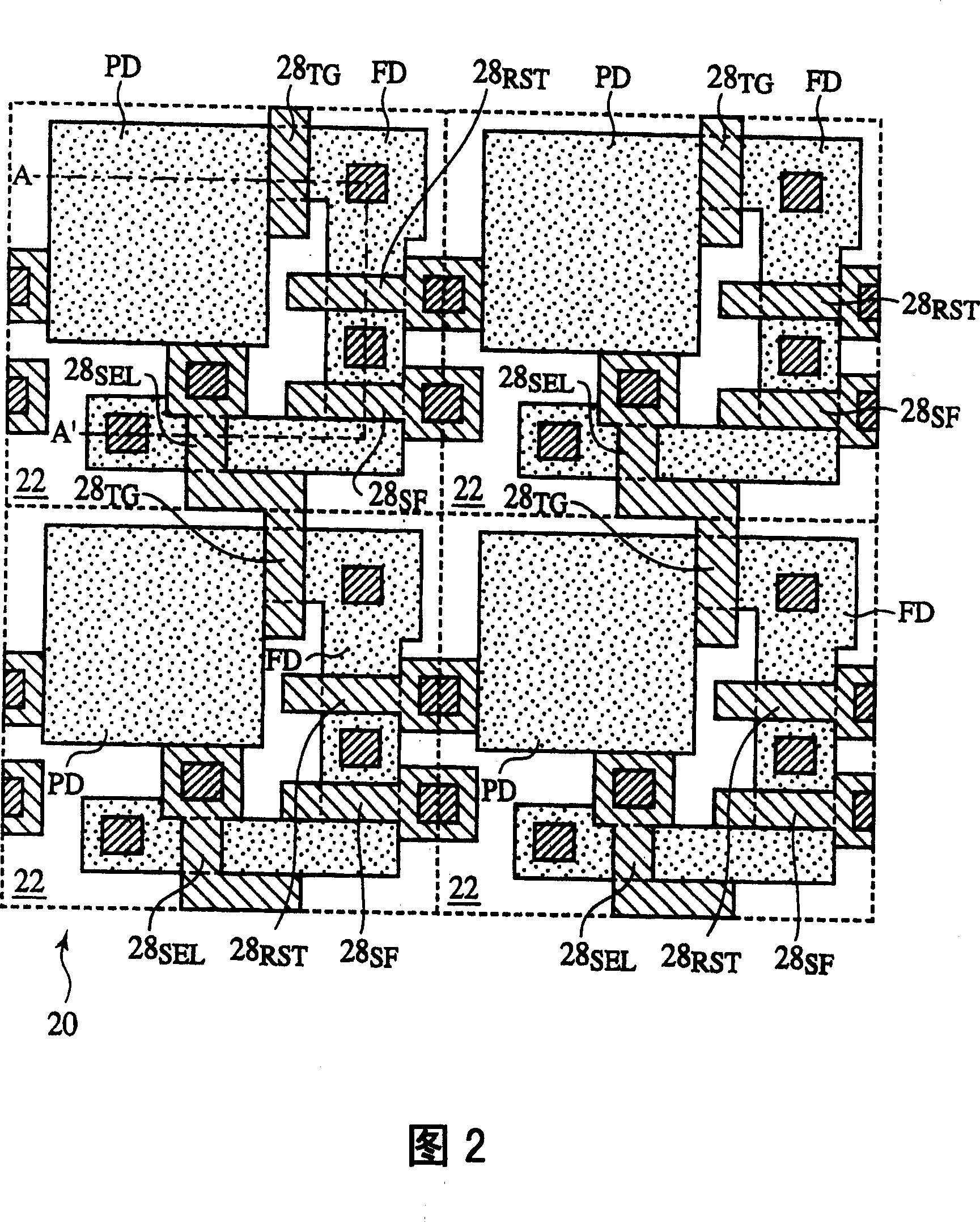
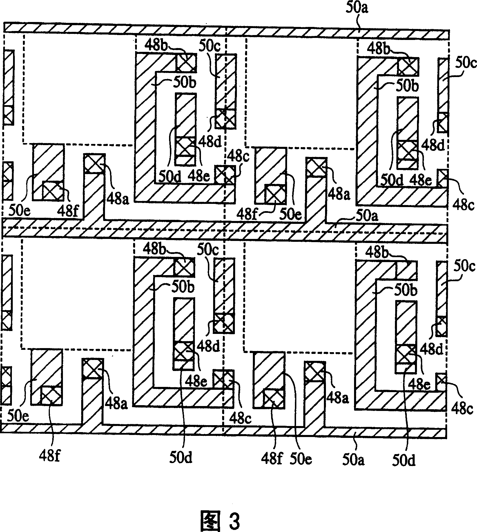
[0057] First, the structure of the solid-state image sensor according to this example will be described with reference to FIGS. 1-5. FIG. 1 is a circuit diagram of a solid-state image sensor according to this example. In FIG. 1, the pixel array unit 10 is represented by a 2×2 uni...

no. 2 example

[0118] A solid-state image sensor according to a second embodiment of the present invention will be described below with reference to FIGS. 9-12.

[0119] 9-12 are plan views showing the structure of the solid-state image sensor according to this example. In order to avoid repetition or simplify description, the same components in this example as in the solid-state image sensor according to the first embodiment shown in FIG. 1 are denoted by the same reference numerals.

[0120] The solid-state image sensor according to this embodiment is the same as the solid-state image sensor according to the first embodiment in circuit diagram, operation, and manufacturing method except that the planar layout of the respective layers is different from that of the solid-state image sensor according to the first embodiment. That is, in the solid-state image sensor according to this example, the TG line commonly connected to the gate terminals of the transfer transistors TG of the respective ...

no. 3 example

[0132] A solid-state image sensor according to a third embodiment of the present invention will be described below with reference to FIGS. 13-16.

[0133] 13-16 are plan views showing the structure of the solid-state image sensor according to this example. In order to avoid repetition or simplify description, the same components in this example as those in the solid-state image sensors according to the first and second embodiments are denoted by the same reference numerals.

[0134] The solid-state image sensor according to this embodiment is the same as the solid-state image sensor according to the first embodiment in terms of circuit diagram, operation, and manufacturing method, except that the layout of individual layers is different from that according to the first embodiment. That is, in the solid-state image sensor according to this example, the TG line commonly connected to the gate terminal of the transfer transistor TG of each pixel in the nth row and the selection tr...


PUM


Abstract

In the solid-state image sensor comprising 4-Tr-pixels, TG lines connecting the gate electrodes 28TG of the transfer transistors of the pixel units of the n row, and select lines connecting the gate electrodes 28SEL of the select transistors of the pixel units of the n+1 row are formed of a common signal line, and the gate electrodes 28TG of the pixels of the n row and the gate electrodes 28SEL of the pixel units of the n+1 row are formed in one continuous pattern of the same conducting layer. Whereby allowance can be given to layouts of the metal interconnection layers. Accordingly, the floating diffusions FD can be effectively shielded from light. Furthermore, allowance can be given to the area. Accordingly, the floating diffusions FD can have the area increased, whereby the junction leakage can be reduced.

Description

field of invention [0001] The present invention relates to a solid-state image sensor and an image reading method, and more particularly to a solid-state image sensor having 4-Tr-pixels and a reading method for such an image sensor. Background technique [0002] A solid-state image sensor mainly composed of CMOS generally adopts a structure called APS (Active Pixel Sensor), which includes a photodiode for converting an optical signal into an electrical signal, a reset transistor for resetting the photodiode, and a photodiode for resetting the photodiode. A source follower transistor that converts the signal charge of the photodiode into a voltage to output the signal charge as a voltage, and a selection transistor for connecting / selecting pixels and a signal line. A solid-state image sensor composed of the above three types of transistors, a so-called 3-Tr-pixel solid-state image sensor, is described in, for example, Reference 1 (Japanese Laid-Open Patent Application No. 200...

Claims


Application Information

Patent Timeline
Patent Type & Authority Patents(China)
IPC IPC(8): H01L27/146H04N5/335H04N5/369H04N5/374
CPCH01L27/14603H01L27/14623H04N3/155H01L27/14643H04N25/766H01L27/146
Inventor 大川成实
Owner FUJITSU MICROELECTRONICS LTD
Why Eureka
Try Eureka