Semiconductor device

A semiconductor and transistor technology, applied in the field of semiconductor devices with transistors, can solve the problems of substrate A20 space waste, increase production cost, etc., achieve the effect of increasing current, reducing production cost, and increasing gate width

Active Publication Date: 2015-04-15
ANCORA SEMICON INC
View PDF4 Cites 2 Cited by
  • Summary
  • Abstract
  • Description
  • Claims
  • Application Information

AI Technical Summary

Problems solved by technology

Electrons hardly flow through the figure 2 The invalid area Z1 in the substrate A20 results in a waste of space on the substrate A20, and the same number of field effect transistors A20 need to be arranged on a substrate A20 with a larger area to output more current, thereby increasing the production cost.

Method used


Image

  • Semiconductor device
  • Semiconductor device
  • Semiconductor device

Examples


Embodiment Construction

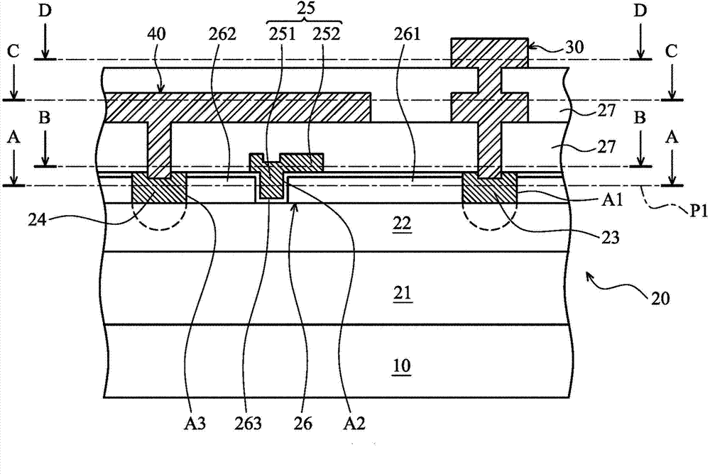
[0056] image 3 It is a cross-sectional view of the semiconductor device 1 of the present invention. Figure 4 for image 3 A cross-sectional view of the AA section. The semiconductor device 1 can be a switching device and can be used in a high-power power supply.

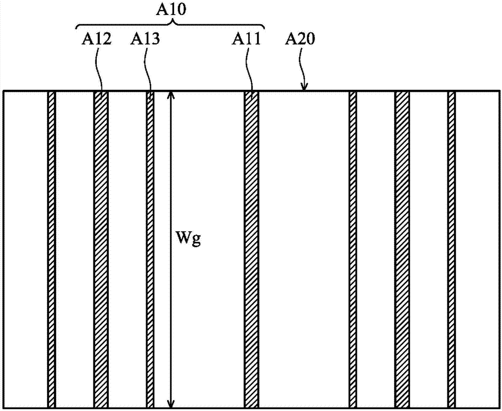
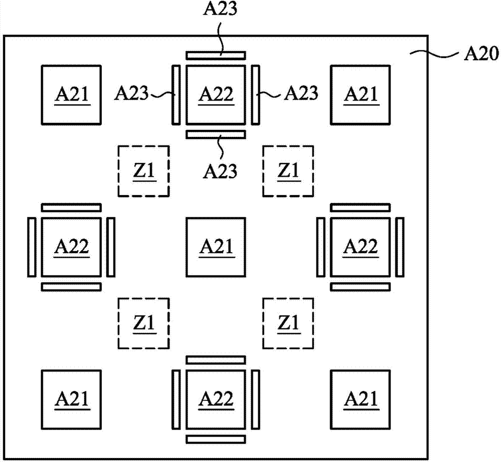
[0057] The semiconductor device 1 includes a substrate 10 , a plurality of transistors 20 , a first conductive layer 30 , and a second conductive layer 40 . The substrate 10 can be a wafer, and its material can be silicon. The transistors 20 may be field effect transistors (FETs) formed on the substrate 10 and may be arranged in an array on the substrate 10 .

[0058] In an embodiment of the present invention, the transistor 20 is a normally-on transistor, which includes a buffer layer 21 , an active layer 22 , a first electrode 23 , a second electrode 24 , and a gate A gate electrode 25 , a protective layer 26 , and an insulating layer 27 are provided. The buffer layer 21 is stacked on the substrate 10 , and...


PUM


Abstract

The invention discloses a semiconductor device. The semiconductor device comprises a substrate and a plurality of transistors arrayed on the substrate. Each transistor comprises a first electrode, a plurality of second electrodes and a grid electrode, wherein the second electrodes are arranged around the first electrode, and the grid electrode is of annular structure and arranged between the first electrode and the second electrodes. The first electrodes and the grid electrodes are circular or polygonal, and the sides of the second electrodes correspond to the shape of the grid electrodes. The semiconductor device can increase output current of the transistors, and invalid area of the substrate is decreased and manufacturing cost is reduced.

Description

technical field [0001] The present invention relates to a semiconductor device, and more particularly, to a semiconductor device having a transistor. Background technique [0002] In order to improve the switching speed of the switch, the current power supply uses a field effect transistor as a switching device. In addition, the field effect transistor also has the advantage of low resistance, which can improve the power supply efficiency of the power supply. [0003] like figure 1 As shown, the conventional field effect transistors A10 are arranged on a substrate A20, and the field effect transistors A10 are connected in parallel with each other, so as to output a larger current. The field effect transistor A10 includes a drain electrode A11, a source electrode A12, and a gate electrode A13. The drain electrode A11, the source electrode A12, and the gate electrode A13 are all linear structures and are parallel to each other. [0004] If the field effect transistor A10 i...

Claims


Application Information

Patent Timeline
Patent Type & Authority Applications(China)
IPC IPC(8): H01L27/088H01L29/423
Inventor 林立凡陈宣文
Owner ANCORA SEMICON INC
Why Eureka
Try Eureka