Metal insulating layer-metal capacitance structure and its manufacturing method

A technology of metal capacitors and manufacturing methods, applied to capacitors, fixed capacitor parts, fixed capacitor dielectrics, etc., can solve problems such as reducing product reliability, peeling, and affecting the electrical function of metal capacitors 26, so as to ensure product reliability. , to avoid the effect of upward or lateral diffusion

Inactive Publication Date: 2008-04-16
UNITED MICROELECTRONICS CORP
View PDF4 Cites 2 Cited by
  • Summary
  • Abstract
  • Description
  • Claims
  • Application Information

AI Technical Summary

Problems solved by technology

[0007] 1. However, the metal lower electrode 14 in the conventional technology is made of copper with poor adhesion to the insulating layer. When the inner metal insulating layer 16 is subsequently formed, it is easy to cause a gap between the metal lower electrode 14 and the inner metal insulating layer 16. The problem of peeling (peeling) occurs
[0008] 2. In addition, the copper ions in the lower metal electrode 14 are very easy to diffuse upward into the inner metal insulating layer 16, or diffuse laterally into the inner metal dielectric layer 20, thereby affecting the electrical performance of the metal capacitor 26. , seriously reducing product reliability

Method used


Image

  • Metal insulating layer-metal capacitance structure and its manufacturing method
  • Metal insulating layer-metal capacitance structure and its manufacturing method
  • Metal insulating layer-metal capacitance structure and its manufacturing method

Examples


Embodiment 1

[0027] refer to Figure 3-Figure 7 Shown is a schematic diagram of a method for forming the metal-insulator-metal (MIM) capacitor structure of the present invention.

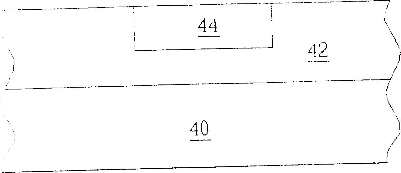
[0028] Such as image 3 As shown, a copper metal layer 44 is disposed in a dielectric layer 42 on a substrate 40 . In the preferred embodiment of the present invention, the copper metal layer 44 is a copper wire in a dual damascene structure (not shown).

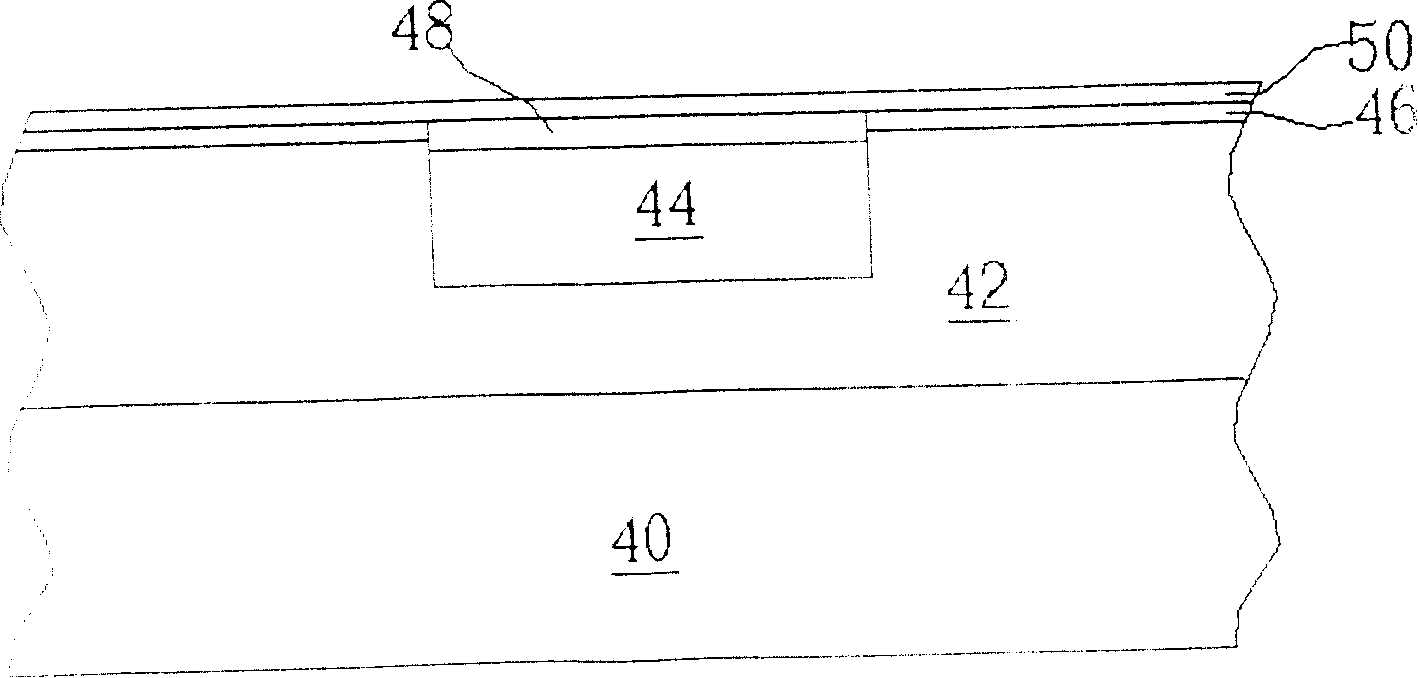
[0029] Such as Figure 4As shown, a sputtering process is first performed to form a first metal layer 46 completely covering the copper metal layer 44 on the copper metal layer 44 . Then perform a rapid thermal oxidation (rapidthermal oxidation, RTO) process, so that the first metal layer 46 in contact with the upper surface of the copper metal layer 44 reacts with the copper metal layer 44 to form an alloy layer 48, and at the same time, it is partially oxidized Or fully oxidize the remaining first metal layer 46 to form a metal oxide layer 50, which cover...

Embodiment 2

[0034] refer to Figure 8 As shown, is a schematic diagram of another embodiment of the MIM capacitor structure 56 of the present invention.

[0035] Such as Figure 8 As shown, the metal oxide layer 50 and the upper pad layer 52 may also only partially cover the alloy layer 48 and the copper metal layer 44 , and the top surface of the alloy layer 48 is roughly aligned with the top surface of the dielectric layer 42 . In subsequent processes, a first via plug 62 and a second via plug 62 may be formed after covering a dielectric layer 66 above the MIM capacitor structure 56 according to product specifications and electrical requirements. The plugs 64 are electrically connected to the upper pad layer 52 and the alloy layer 48 not covered by the metal oxide layer 50 . Since the formation methods and functions of the first metal layer 46 , the alloy layer 48 , the metal oxide layer 50 and the upper pad layer 52 in the second embodiment are the same as those in the preferred embo...


PUM


Abstract

A capacitor with the metal-insulating layer-metal structure is sequentially composed of a copper layer in a dielectric layer on substrate, an alloy layer above said copper layer, a metallic oxide layer on said alloy layer, and an upper pad layer above the metallic oxide layer, Its advantages are no diffusion of copper ions, and high electric properties and reliability.

Description

technical field [0001] The invention provides a metal-insulator-metal (MIM) capacitor structure, in particular to a metal-insulator-metal (MIM) capacitor structure including copper electrodes and a manufacturing method thereof. Background technique [0002] As we all know, in the semiconductor process, metal capacitors composed of metal layer, insulating layer, metal layer (MIM) composite structure have been widely used in the design of semiconductor elements. Because this kind of metal capacitor has a lower resistance value (resistance) and a smaller parasitic capacitance (parasitic capacitance), and there is no problem of depletion layer induced voltage (induced voltage) shift, so the MIM structure is mostly used as a metal capacitor at present. main structure. In particular, MIM capacitors with low-resistance copper electrodes are the focus of current research. [0003] Referring to FIGS. 1-2 , they are schematic diagrams of a conventional method for fabricating a metal...

Claims


Application Information

Patent Timeline
Patent Type & Authority Patents(China)
IPC IPC(8): H01G4/10H01L27/10H01L21/82H01L21/02
CPCH01L28/75
Inventor 李秋德
Owner UNITED MICROELECTRONICS CORP
Why Eureka
Try Eureka