
Chip checking system and method

An inspection system and inspection method technology, applied in electrical components, semiconductor/solid-state device manufacturing, semiconductor/solid-state device testing/measurement, etc., can solve the problems of product quality damage, futile follow-up processes, inconvenient inspection, etc., to improve the finished product. efficiency, shortening inspection time, and reducing process burden

Inactive Publication Date: 2008-04-16
POWERCHIP SEMICON CORP
View PDF3 Cites 0 Cited by
  • Summary
  • Abstract
  • Description
  • Claims
  • Application Information

AI Technical Summary

Problems solved by technology

[0003] Defects on the back of the crystal, such as scratches, particles, missing corners, and cracks, can easily cause many problems
For example, the particles attached to the back of the crystal will make the wafer less likely to be absorbed by the suction cup, or cause the graphics of the yellow light process to be out of focus; scratches, missing corners, and cracks on the back of the crystal are precursors of process machine failures, which will lead to expensive of the wafers suffered continuous product quality damage or fragmentation during the process
Therefore, if the problematic machine cannot be found in real time, the loss will be enlarged or the entire batch of wafers will be scrapped, making the follow-up process futile and resulting in a decline in product yield
[0004] At present, the industry uses a wafer flipper to inspect the crystal back. However, the wafer flipper needs an extra long time to flip the wafer, which doubles the time of the entire visual inspection operation.
Moreover, the jig used by the flipper to absorb the wafer will also cover some areas on the edge of the crystal back, so that these covered areas cannot be inspected, but these areas are often important areas that are prone to defects on the crystal back, so it will cause defects. inspection inconvenience

Method used


Image

  • Chip checking system and method
  • Chip checking system and method
  • Chip checking system and method

Examples


Embodiment Construction

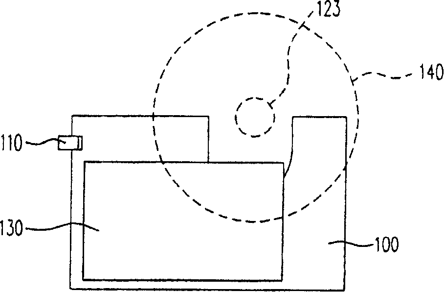
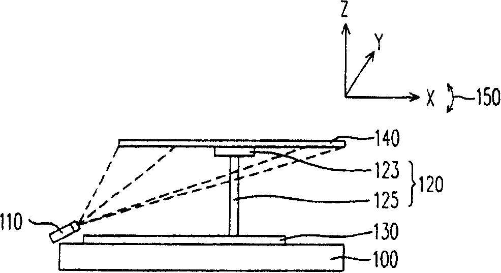
[0033] Figure 1A It is a top view of a wafer inspection system according to an embodiment of the present invention. Figure 1B It is a side view of a wafer inspection system according to an embodiment of the present invention when inspecting wafers.

[0034] Please refer to Figure 1A and Figure 1B , the present invention proposes a wafer inspection system, which is composed of, for example, a light source 110 , a wafer carrier 120 and a reflective element 130 . The wafer carrying device 120 is used for carrying a wafer 140 . The light source 110 is configured corresponding to the wafer carrier 120 , for example, it is disposed beside the wafer carrier 120 to illuminate the backside of the wafer 140 . The reflective element 130 is configured corresponding to the wafer carrier 120 , for example, is disposed under the wafer carrier 120 to reflect the backside of the wafer 140 .

[0035] Wherein, the light source 110 is, for example, a light emitting diode, an organic light ...


PUM


Abstract

The invention is concerned with the wafer visual examination method, it is: provides a wafer visual examination system that is at least consist of the loading equipment, the photosource and the reflection component; the wafer loading equipment is used to load wafer; the photosource is configured corresponding with the loading equipment in order to light the back of the wafer; the reflection component is configured corresponding with the loading equipment and uses the photosource to light the back of the wafer; exams the wafer back that shines by the wafer surface and the reflection component.

Description

technical field [0001] The invention relates to a semiconductor process equipment, in particular to a wafer visual inspection system and a wafer inspection method using the wafer visual inspection system. Background technique [0002] Today, with the rapid development of integrated circuits, tens of thousands of electronic components are often formed on a single chip. In order to ensure the quality of the process, most of the industry will inspect the crystal surface to detect defects early and remedy them as soon as possible. As the semiconductor industry enters the deep sub-micron process, in addition to the inspection of the crystal surface, the inspection of the crystal back is also increasingly valued. [0003] Defects on the crystal back, such as scratches, particles, missing corners, and cracks, can easily cause many problems. For example, the particles attached to the back of the crystal will make the wafer less likely to be absorbed by the suction cup, or cause the...

Claims


Application Information

Patent Timeline
Patent Type & Authority Patents(China)
IPC IPC(8): H01L21/66H01L21/68
Inventor 刘国忠陈镡笙戴景松邱任川
Owner POWERCHIP SEMICON CORP
Learn More