


Quick Research
Generate reliable direction feasibility study reports for your R&D in just a few steps.

Technical Q&A
Discover and master advanced knowledge NOW. Basics, ideas, possibilities, all at once.

Find Solutions
As an expert in R&D theories, this can generate solutions to your technical problems instantly.

Evaluate Feasibility
Analyze your overall solution with one click, know your potential R&D risks in advance.

Monitor Landscape
Get weekly tech updates, stay abreast of the latest tech innovations and key insights.
Electric charge detecting apparatus
一种电荷、导电型的技术,应用在辐射控制装置、电视、电路等方向,能够解决变动变大、电容Cfd变化量变大、输出电压动态范围变窄等问题,达到依存性小、动态范围大、线性好的效果
- Summary
- Abstract
- Description
- Claims
- Application Information
AI Technical Summary
Problems solved by technology
Method used
Image

Examples
Embodiment 1
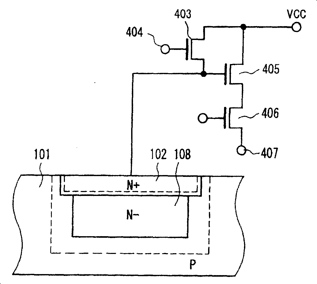
[0029] Figure 1A It is a diagram showing the semiconductor cross-sectional structure and the configuration of the output circuit of the photoelectric conversion portion of the charge detection device according to the first embodiment of the present invention. In addition, in Figure 1A Among them, for those with reference to the existing examples Figure 4A Parts with the same configuration and function are attached with the same symbols and their descriptions are omitted. In addition, the dotted line in the drawing indicates the end of the depletion layer.
[0030] The photoelectric conversion part is constituted by forming a photodiode N layer 108 on a P-type semiconductor substrate (or P well) 101, and forming a photodiode N layer 102 thereon so that the impurity concentration of the surface becomes high. In addition, this photoelectric conversion part also functions as a charge storage part and a diffusion drift region, and is connected to the gate of the amplifier MOS ...
Embodiment 2
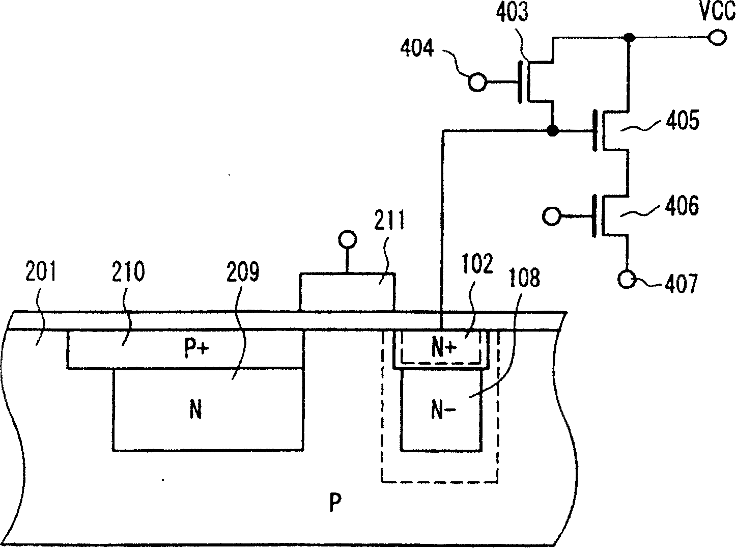
[0043] figure 2 It is a diagram showing a cross-sectional structure of a semiconductor and a configuration of an output circuit in a case where the charge detection device of the first embodiment is applied to the sensor of the solid-state imaging device CCD according to the second embodiment of the present invention. In addition, in figure 2 , for having the same as that referred to in the description of Example 1 Figure 1A Parts with the same configuration and function are attached with the same symbols and their descriptions are omitted. In addition, the dotted line in the drawing indicates the end of the depletion layer.
[0044] exist figure 2 Among them, the photodiode uses the buried type, and the surface of the N layer 209 of the photodiode commonly used in the CCD sensor is formed of the high-concentration P-type 210 . The low-voltage, high-sensitivity charge-to-voltage conversion unit according to Embodiment 1 is connected to the output circuit through the re...
Embodiment 3
[0046] image 3 It is a diagram showing the semiconductor cross-sectional structure and the configuration of the output circuit of the photoelectric conversion part of the charge detection device according to the third embodiment of the present invention. In addition, in image 3 , for having the same as that referred to in the description of Example 1 Figure 1A Parts with the same configuration and function are attached with the same symbols and their descriptions are omitted. In addition, the dotted line in the drawing indicates the end of the depletion layer.
[0047] This embodiment is an example of a further improvement on the configuration of Embodiment 1. The most important thing in the present invention is to prefer a low-concentration N-layer region. The low-concentration N-layer region consists of two regions. The N layer region with low concentration on the surface side (N - ) 308a is formed such that the impurity concentration is lower than that of the low-co...
PUM
 Abstract
Description
Claims
Application Information
 - R&D Engineer
- R&D Manager
- IP Professional
- Industry Leading Data Capabilities
- Powerful AI technology
- Patent DNA Extraction
Browse by: Latest US Patents, China's latest patents, Technical Efficacy Thesaurus, Application Domain, Technology Topic, Popular Technical Reports.
© 2024 PatSnap. All rights reserved.Legal|Privacy policy|Modern Slavery Act Transparency Statement|Sitemap|About US| Contact US: help@patsnap.com